Iintegrated circuit device including asymmetrical fin field-effect transistor

Active Publication Date: 2019-02-28
SAMSUNG ELECTRONICS CO LTD
View PDF1 Cites 4 Cited by
  • Summary
  • Abstract
  • Description
  • Claims
  • Application Information

AI Technical Summary

Benefits of technology

[0004]The present disclosure provides an integrated circuit device in which electrical shorts between adjacen

Problems solved by technology

Down-scaling of integrated circuit devices may cause a short channel effect

Method used


Image

  • Iintegrated circuit device including asymmetrical fin field-effect transistor
  • Iintegrated circuit device including asymmetrical fin field-effect transistor
  • Iintegrated circuit device including asymmetrical fin field-effect transistor

Examples


Embodiment Construction

[0016]Hereinafter, embodiments of the inventive concept will be described in detail with reference to the accompanying drawings.

[0017]As used herein, an integrated circuit device may refer, for example, to a transistor or a device such as a semiconductor chip (e.g., memory chip and / or logic chip formed from a wafer), a stack of semiconductor chips, a semiconductor package including one or more semiconductor chips stacked on a package substrate, or a package-on-package device including a plurality of packages. These devices may be formed using ball grid arrays, wire bonding, through substrate vias, or other electrical connection elements, and may include memory devices such as volatile or non-volatile memory devices.

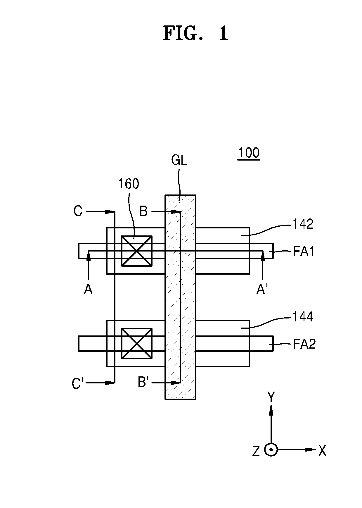
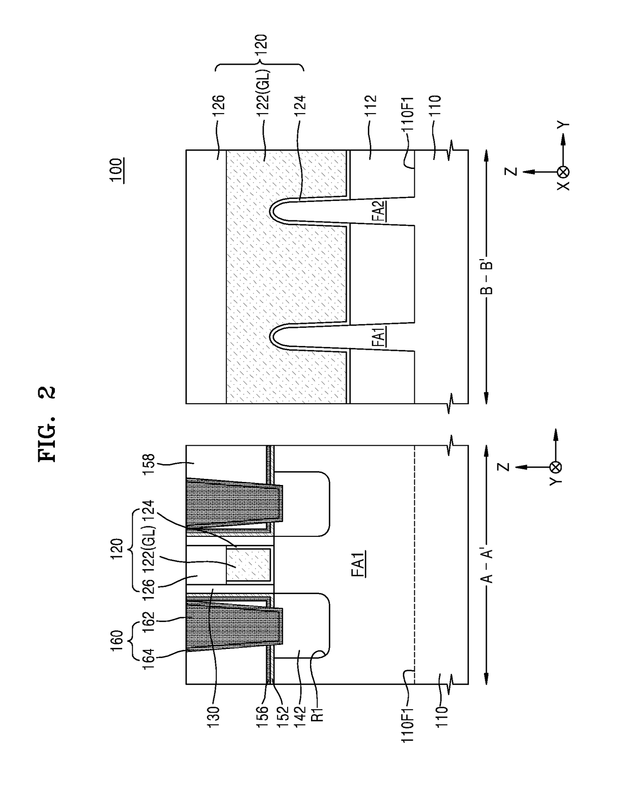
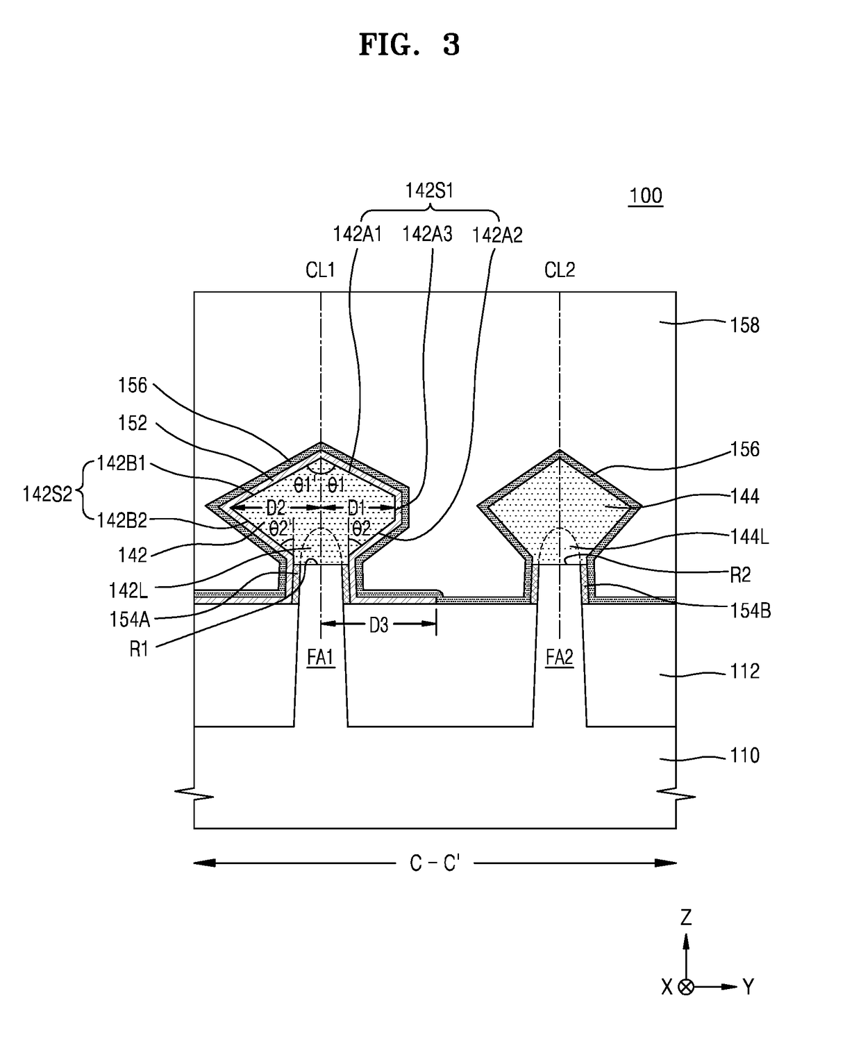
[0018]FIG. 1 is a layout diagram illustrating an integrated circuit device 100 according to an example embodiment. FIG. 2 shows cross-sectional views taken along line A-A′ and line B-B′ in FIG. 1, respectively according to example embodiments. FIG. 3 is a cross-sectional ...


PUM


Abstract

An integrated circuit device includes: a first fin active region extending in a first direction parallel to a top surface of a substrate; a second fin active region extending in the first direction and spaced apart from the first fin active region in a second direction different from the first direction; a gate line intersecting the first and second fin active regions; a first source/drain region on one side of the gate line in the first fin active region; and a second source/drain region on one side of the gate line in the second fin active region and facing the first source/drain region, wherein a cross-section of the first source/drain region perpendicular to the first direction has an asymmetric shape with respect to a center line of the first source/drain region in the second direction extending in a third direction perpendicular to the top surface of the substrate.

Description

CROSS-REFERENCE TO RELATED APPLICATION[0001]This application claims the benefit of Korean Patent Application No. 10-2017-0106255, filed on Aug. 22, 2017, in the Korean Intellectual Property Office, the disclosure of which is incorporated herein in its entirety by reference.BACKGROUND[0002]The present disclosure relates to an integrated circuit device, and more particularly, to an integrated circuit device including a fin active region.[0003]There is a growing demand for high integration of integrated circuit devices according to a tendency of electronic products to be thinner and smaller. Down-scaling of integrated circuit devices may cause a short channel effect of transistors, which reduces the reliability of integrated circuit devices. In order to reduce the short channel effect, an integrated circuit device including a fin active region has been proposed. In addition, as the design rule decreases, sizes of components of the integrated circuit device and distance therebetween are...

Claims


Application Information

Patent Timeline
IPC IPC(8): H01L29/66H01L29/78H01L29/08H01L21/8238H01L21/8234H01L21/02H01L21/308
CPCH01L29/66795H01L21/823418H01L21/823431H01L21/823821H01L21/3083H01L21/02532H01L21/02576H01L21/02579H01L21/02598H01L21/02634H01L21/02639H01L29/0847H01L29/78H01L21/823814H01L21/823878H01L27/0924H01L29/7854H01L21/0262H01L29/66545H01L29/165H01L29/7848H10B10/18H10B10/12H01L27/0886H01L29/7855H01L29/7835H01L27/10
Inventor CHO, EDWARD NAMKYULIM, BO-RASEONG, GEUM-JUNGLEE, SEUNG-HUN
Owner SAMSUNG ELECTRONICS CO LTD
Why Eureka
Try Eureka