Vertical memory devices and methods of manufacturing the same

a technology of vertical memory and manufacturing method, which is applied in the direction of semiconductor devices, semiconductor/solid-state device details, electrical apparatus, etc., can solve the problems of hole penetration through gate electrodes, and achieve the effect of reducing contact resistance and preventing electrical shorts between gate electrodes formed on different levels

Active Publication Date: 2020-02-06
SAMSUNG ELECTRONICS CO LTD
View PDF3 Cites 8 Cited by
  • Summary
  • Abstract
  • Description
  • Claims
  • Application Information

AI Technical Summary

Benefits of technology

[0011]In a vertical memory device in accordance with an example embodiment of the present inventive concept, contact plugs formed to contact each of gate electrodes stacked in a vertical direction may be formed in the corresponding gate electrodes without extending through the corresponding gate electrodes, the contact resistance may be reduced, and electrical short between the gate electrodes formed on different levels may be prevented.

Problems solved by technology

However, when the thicknesses of the gate electrodes are small, the holes may penetrate through the gate electrodes.

Method used


Image

  • Vertical memory devices and methods of manufacturing the same
  • Vertical memory devices and methods of manufacturing the same
  • Vertical memory devices and methods of manufacturing the same

Examples


Embodiment Construction

[0017]Example embodiments of the present inventive concept will be more clearly understood from the following detailed description taken in conjunction with the accompanying drawings.

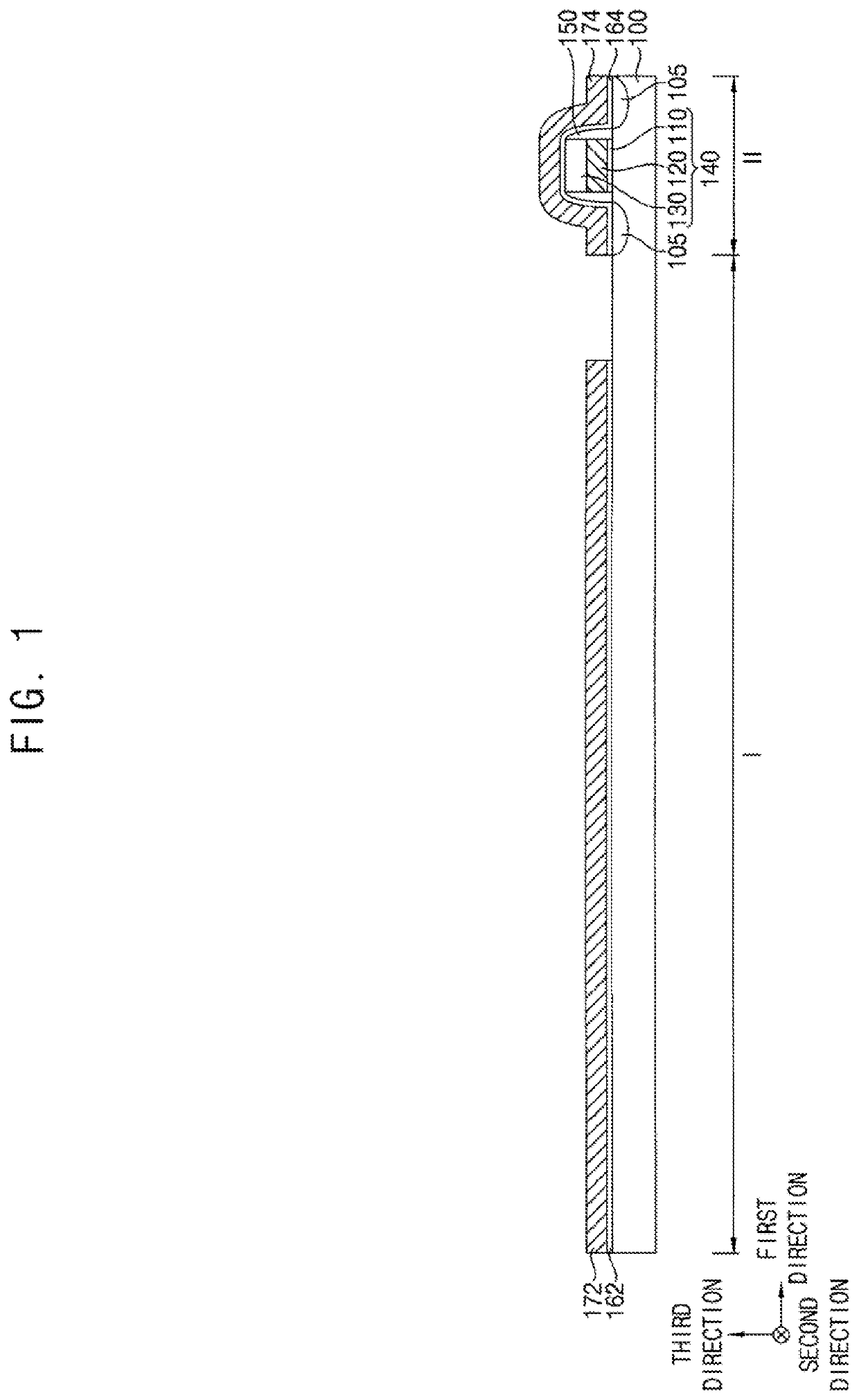
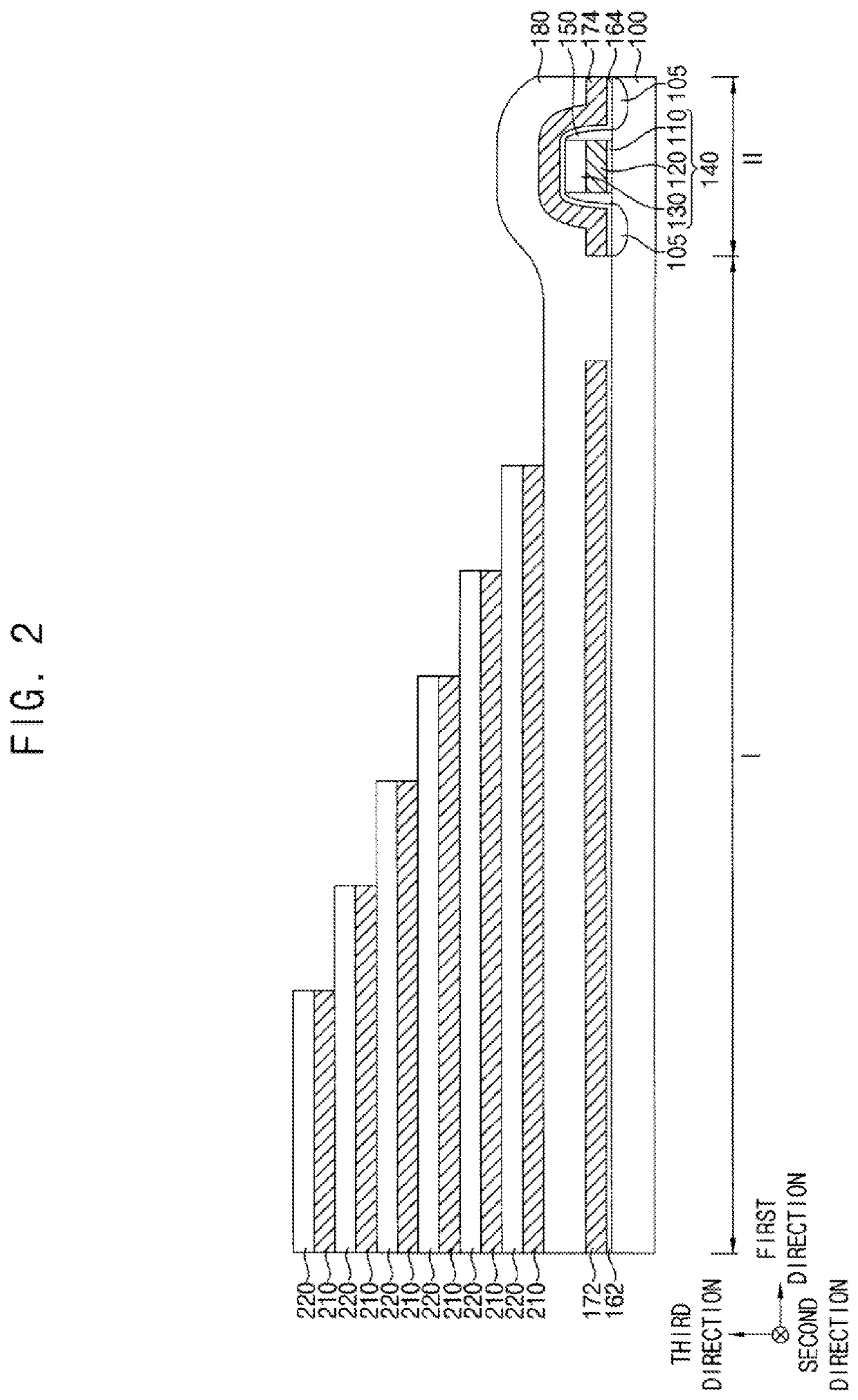
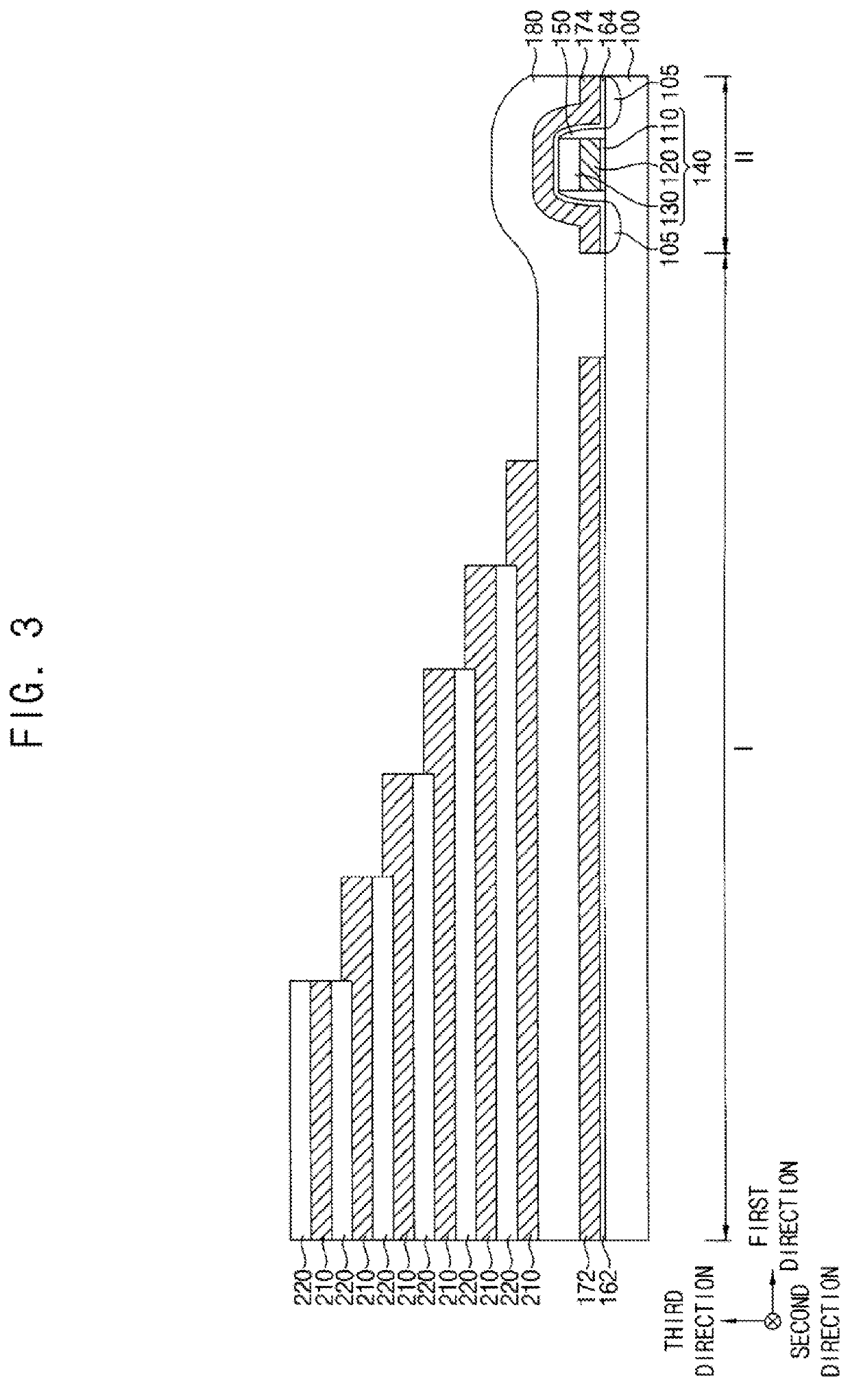
[0018]FIGS. 1 to 14 are cross-sectional views illustrating a method of manufacturing a vertical memory device in accordance with an example embodiment of the present inventive concept. FIGS. 11 and 13 are enlarged cross-sectional views of X regions of FIGS. 10 and 12, respectively.

[0019]Hereinafter, two directions intersecting with each other among horizontal directions substantially parallel to an upper surface of a substrate are defined as first and second directions, respectively, and a vertical direction substantially perpendicular to the upper surface of the substrate is defined as a third direction. In an example embodiment of the present inventive concept, the first and second directions may be orthogonal to each other. The third direction may be substantially perpendicular to the first and secon...


PUM

PropertyMeasurementUnit
dielectric constantaaaaaaaaaa
thicknessaaaaaaaaaa

Abstract

A vertical memory device includes first gate electrodes stacked on a cell region of a substrate and spaced apart from each other in a vertical direction substantially perpendicular to an upper surface of the substrate, a channel extending through the first gate electrodes and extending in the vertical direction, a first contact plug structure contacting a corresponding one of the first gate electrodes, extending in the vertical direction, and including a first metal pattern, a first barrier pattern covering a lower surface and a sidewall of the first metal pattern and a first metal silicide pattern covering a lower surface and a sidewall of the first barrier pattern, and a second contact plug structure extending in the vertical direction on a peripheral circuit region of the substrate and including a second metal pattern and a second barrier pattern covering a lower surface and a sidewall of the second metal pattern.

Description

CROSS-REFERENCE TO RELATED APPLICATION[0001]This application claims priority under 35 U.S.C. § 119 to Korean Patent Application No. 10-2018-0090766, filed on Aug. 3, 2018, in the Korean Intellectual Property Office (KIPO), the contents of which are herein incorporated by reference in their entirety.TECHNICAL FIELD[0002]Example embodiments of the present inventive concept relate to a vertical memory device and a method of manufacturing the same.DISCUSSION OF RELATED ART[0003]In a process of fabricating a vertical NAND (VNAND) flash memory device, holes may be formed to expose gate electrodes on a cell region of a substrate, and metal patterns may fill the holes to form contact plugs, which may be connected to the gate electrodes, respectively. However, when the thicknesses of the gate electrodes are small, the holes may penetrate through the gate electrodes.SUMMARY[0004]Example embodiments of the present inventive concept provide a vertical memory device having enhanced electrical ch...

Claims


Application Information

Patent Timeline
Patent Type & Authority Applications(United States)
IPC IPC(8): H01L27/11582H01L29/423H01L23/535H01L27/11573H01L29/45
CPCH01L29/4234H01L27/11582H01L29/456H01L27/11573H01L23/535H10B41/41H10B41/35H10B41/27H01L21/76858H01L21/76843H01L21/76816H10B43/50H10B43/40H10B43/27H10B43/35H01L29/66666H01L21/823487H01L21/76897H01L21/76841
Inventor KANG, SHIN-HWANSHIM, SUN-ILHYUN, SEUNG
Owner SAMSUNG ELECTRONICS CO LTD
Why Eureka
Try Eureka