Multilayer wiring board and fabricating method of the same

a wiring board and multi-layer technology, applied in the direction of thermoplastic polymer dielectrics, dielectric characteristics, printed circuit non-printed electric components association, etc., can solve the problems of buckling of the connection site itself, inability to re-melt alloy, and inability to affect the connection process. , to achieve the effect of high connection stability

Inactive Publication Date: 2006-12-07
SONY CORP
View PDF8 Cites 29 Cited by
  • Summary
  • Abstract
  • Description
  • Claims
  • Application Information

AI Technical Summary

Benefits of technology

[0027] Further, existence of the binder resin makes the structure of the alloy in the via hole uniform. As a result, it is possible to obtain a multilayer wiring board having high connection stability.

Problems solved by technology

In the above connection mechanism, however, the following problem may arise at the conductive composition formation time by sintering.
Therefore, it is not possible to re-melt the alloy 103 for compression, with the result that voids remain in the via metal.
If compression is continued in such a case, the connection site itself may be subjected to buckling to affect the connection process.
If compression is continued in such a state, a pattern formed in the vicinity of via holes may be broken to generate cracks.
However, this method takes a long time, failing to take advantage of the properties of the thermoplastic resin that melting and boding lamination process can be done at short times. As a result, productivity decreases to increase cost.

Method used


Image

  • Multilayer wiring board and fabricating method of the same
  • Multilayer wiring board and fabricating method of the same
  • Multilayer wiring board and fabricating method of the same

Examples


Embodiment Construction

[0036] An embodiment of the present invention will be described in detail with reference to the accompanying drawings.

[0037] Structure of Multilayer Wiring Board

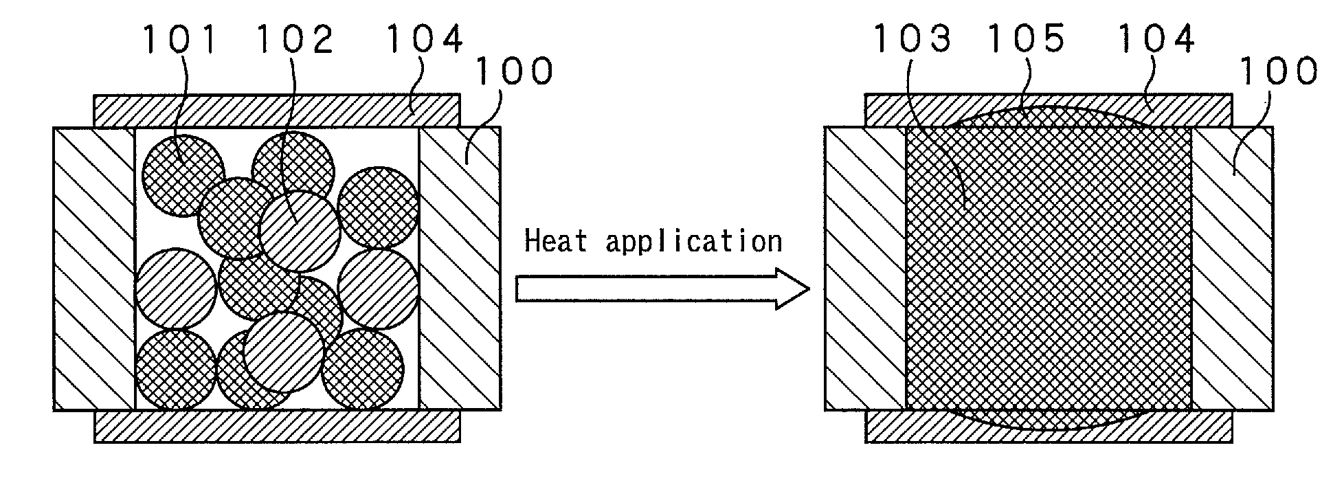
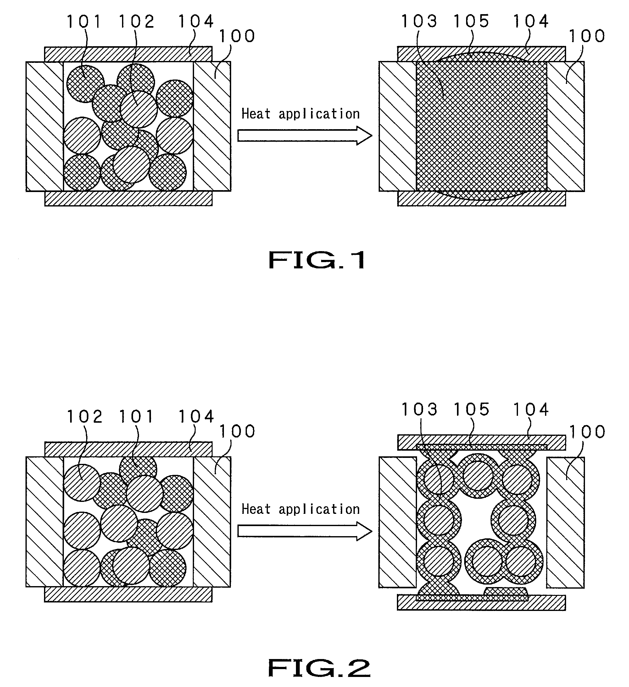
[0038]FIG. 3 is a view schematically showing the cross-section of a multilayer wiring board 10 according to an embodiment of the present invention.

[0039] As shown in FIG. 3, the multilayer wiring board 10 includes a base material 11 and metal conductor patterns 12 (12a, 12b) formed on both sides (upper and lower surfaces) of the base material 11. A via hole 13 penetrating the base material 11 from the upper surface to lower surface thereof is formed in the base material 11. An interlayer connection part 14 is formed in the via hole 13. The upper and lower openings of the via hole 13 are covered by the conductor patterns 12 (12a, 12b). The interlayer connection part 14 is connected to the conductor patterns 12 (12a, 12b) formed on both sides of the base material 11 and electrically connects the conductor patterns 12 and ba...


PUM

PropertyMeasurementUnit
temperatureaaaaaaaaaa
melting pointaaaaaaaaaa

Abstract

To improve reliability of interlayer connection of a multilayer wiring board. Plural metal conductor pattern layers are formed on a base material made of thermoplastic resin. Then, high melting metal containing copper, low melting metal containing tin, and binder resin are packed into a via hole. Subsequently, predetermined heat and pressure are applied. Then, while half-melted metal mixture droplets of the low and high melting metals and melted binder resin are phase separated from each other, the surfaces of the conductor patterns that face the openings of the via and the low melting metal are alloyed with each other to form an alloy layer as well as the high and low meting metals are alloyed with each other to form a columnar-shaped interlayer connection part. As a result, an intermediate layer is formed between the outer surface of the columnar-shaped interlayer connection part and inner surface of the via hole.

Description

CROSS REFERENCE TO RELATED APPLICATIONS [0001] The present invention contains subject matter related to Japanese Patent Applications JP 2004-325259 and JP 2005-212570 filed in Japanese Patent Office on Nov. 9, 2004, and Jul. 22, 2005, the entire contents of which being incorporated herein by reference. BACKGROUND OF THE INVENTION [0002] 1. Field of the Invention [0003] The present invention relates to a multilayer wiring board in which a plurality of metal conductor pattern layers are formed on a base material made of a thermoplastic resin and a method of fabricating the same. [0004] 2. Description of the Related Art [0005] Along with the widespread use of portable electronic devices such as a mobile phone, a digital still camera, build-up boards have come to the forefront in the market. The build-up boards are designed to realize ultra-miniaturization of components as well as a fine pattern or miniaturization of via hole sizes for high-density implementation. However, the build-up ...

Claims


Application Information

Patent Timeline
Patent Type & Authority Applications(United States)
IPC IPC(8): H05K7/00H01R43/00
CPCH05K3/4069H05K3/4617H05K3/4632H05K2201/0129Y10T29/49117H05K2201/0394H05K2203/0425H01R12/523H05K2201/0141
Inventor NAKADA, MASAKAZUOGAWA, MINORU
Owner SONY CORP
Why Eureka
Try Eureka