Supercharge Your Innovation With Domain-Expert AI Agents!

Method and system for writing physical blocks

A physical block and physical page technology, applied in the direction of input/output to record carrier, memory address/allocation/relocation, etc., can solve the problem that the number of data integration does not decrease, data integration consumes the number of reads and writes of NAND chips, and shortens NAND chips Effective service life and other issues to achieve the effect of reducing the number of times and prolonging the service life

Active Publication Date: 2014-08-06
ANYKA (GUANGZHOU) MICROELECTRONICS TECH CO LTD
View PDF1 Cites 2 Cited by
  • Summary
  • Abstract
  • Description
  • Claims
  • Application Information

AI Technical Summary

Problems solved by technology

And in the case of multiple buffer blocks, it is likely that the sector corresponding to the physical page in the buffer block written later completely contains the sectors contained in the corresponding physical page in the buffer block written earlier, so the first written All data in the buffer block is invalid and does not need to be sorted into data blocks, that is, the buffer block written first is completely invalid in this case
However, in the prior art, the above-mentioned invalid buffer blocks still need to be kept until the end of the entire writing process, and there are a large number of invalid buffer blocks in the process of sorting data into new data blocks, so that the number of times of data integration is not reduced to a minimum. Excessive data integration consumes the number of reads and writes of the NAND chip, shortening the effective life of the NAND chip

Method used


Image

  • Method and system for writing physical blocks
  • Method and system for writing physical blocks
  • Method and system for writing physical blocks

Examples


Embodiment Construction

[0045] In order to make the purpose, technical solutions and advantages of the embodiments of the present invention clearer, the technical solutions in the embodiments of the present invention will be clearly and completely described below in conjunction with the drawings in the embodiments of the present invention. Obviously, the described embodiments It is a part of embodiments of the present invention, but not all embodiments. Based on the embodiments of the present invention, all other embodiments obtained by persons of ordinary skill in the art without making creative efforts belong to the protection scope of the present invention.

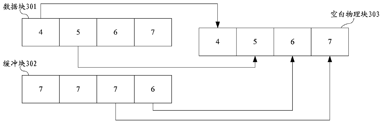
[0046] The invention provides a method for writing physical blocks, which is mainly used in NAND chips. In the writing method of the present invention, the existing writing method is optimized, so that the method can find invalid buffer blocks, and release the mapping relationship between invalid buffer blocks and logic blocks. For the conve...


PUM


Abstract

The embodiment of the invention provides a method for writing physical blocks. The method comprises the following specific steps: a, establishing a mapping relation of logic blocks and the physic blocks; b, sequentially writing data in buffer blocks and finishing the writing of n buffer blocks; c, contrasting the kth buffer block to all buffer blocks written after the kth buffer block is written, judging whether a sector range corresponding to the buffer blocks written after the kth buffer block is written covers a sector range corresponding to the kth buffer block or not, if so, determining the kth buffer block to be an invalid buffer block, and otherwise, determining the kth buffer block to be a valid buffer block; terminating the mapping relation of the invalid buffer blocks and the logic blocks; d, selecting the physical blocks of which the quantity is equal to that of the invalid buffer blocks as buffer blocks and finishing the writing of newly-selected buffer blocks; e, repeatedly executing the steps from c to d until the n buffer blocks are valid buffer blocks respectively and searching valid data from original data blocks and the valid buffer blocks; copying all valid data to new data blocks, wherein k is an integer which is greater than 0 and is smaller than n.

Description

technical field [0001] The invention relates to the technical field of data storage, in particular to a method and system for writing physical blocks. Background technique [0002] NAND is a flash memory solution with excellent performance at the current stage. It is characterized by low power consumption, light weight, and good read and write performance; it is currently widely used in flash disks and memory cards. As a storage medium, a NAND chip includes multiple physical blocks, and each physical block includes multiple physical pages. Because the number of erasing and writing of physical blocks and physical pages of NAND chips is limited, the write balance algorithm derived from this has become an important technical means to prolong the service life of NAND chips. The write balance algorithm is usually based on the mapping relationship between the logical block or sector in the virtual layer of the file system and the actual physical block or physical page of the NAND...

Claims


Application Information

Patent Timeline
IPC IPC(8): G06F12/06G06F3/06
Inventor 李晓辉黄亮杨汉森胡胜发
Owner ANYKA (GUANGZHOU) MICROELECTRONICS TECH CO LTD
Features
  • R&D
  • Intellectual Property
  • Life Sciences
  • Materials
  • Tech Scout
  • Unparalleled Data Quality
  • Higher Quality Content
  • 60% Fewer Hallucinations
Learn More