Supercharge Your Innovation With Domain-Expert AI Agents!

Pixel structure and manufacturing method and repair method thereof

A technology of pixel structure and manufacturing method, applied in nonlinear optics, instruments, optics, etc., can solve problems such as poor repair effect, long wiring lines, input signal delay distortion, etc., to achieve the effect of line defect repair

Active Publication Date: 2014-08-13
NANJING CEC PANDA LCD TECH
View PDF5 Cites 19 Cited by
  • Summary
  • Abstract
  • Description
  • Claims
  • Application Information

AI Technical Summary

Problems solved by technology

Due to the long routing of the ring winding around the panel display area, the delay and distortion of the input signal are caused, and the repair effect is not good.

Method used


Image

  • Pixel structure and manufacturing method and repair method thereof
  • Pixel structure and manufacturing method and repair method thereof
  • Pixel structure and manufacturing method and repair method thereof

Examples


Embodiment 1

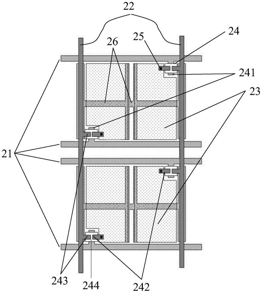
[0074] Figure 5 It is a schematic diagram of repairing a broken scanning line of a double-gate pixel structure including H-shaped repairing lines according to an embodiment of the present invention. Such as Figure 5 As shown, in the pixel structure driven by double gates, an H-shaped repair line structure is designed between the upper row of pixels and the lower row of pixels. The scan lines of a row of pixels overlap.

[0075] Such as Figure 5 With the pixel structure driven by double gates shown, when a breakpoint 53 occurs in the scan line 51, the corresponding repair method is as follows:

[0076] a. On the scan line 51 where the disconnection occurs, find the area where the H-shaped repair line 57 on the left and right sides of the breakpoint 53 overlaps with the scan line 51 .

[0077] b. Laser welding is performed on the overlapping areas on both sides of the break point respectively to form welding points 521 and 522 .

[0078] After laser welding, the voltage ...

Embodiment 2

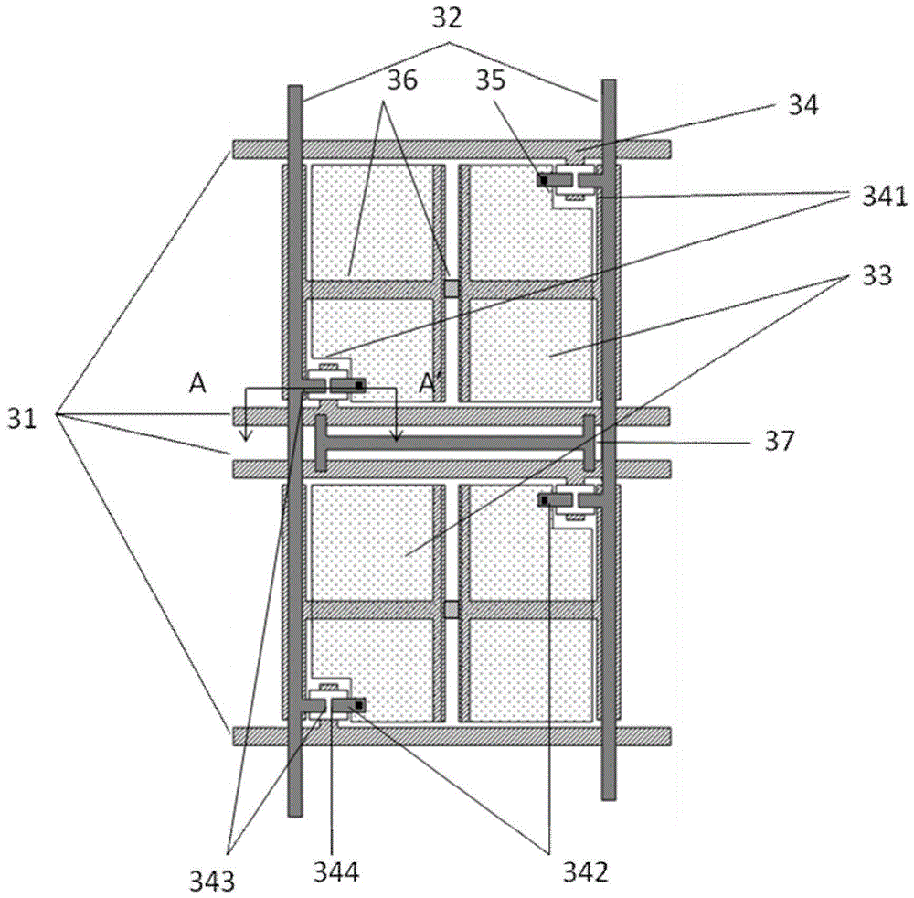
[0080] Image 6 It is a schematic diagram of repairing a broken scan line of a double-gate pixel structure including a "Feng"-shaped repair line according to an embodiment of the present invention. Such as Image 6 As shown, in the pixel structure driven by double gates, a "Feng" font is designed between the upper row of pixels and the lower row of pixels, and between the right pixel of the left data line and the left pixel of the right data line The repair line structure, the "Feng" font repair line structure is a simultaneous electrical connection of the upper and lower H-shaped repair line structures through the connection line between the right pixel of the left data line and the left pixel of the right data line. layer metal structure. In the H-shaped repair line structure in the "Feng"-shaped repair line structure, the bottom of both sides is designed with the same layer of repair liners as the scan line. Both ends of the repair liner have partial overlapping regions ...

Embodiment 3

[0086] Figure 7 It is a schematic diagram of data line broken line repairing in a dual-gate pixel structure including "Feng"-shaped repairing lines according to an embodiment of the present invention. Such as Figure 7 As shown, in the pixel structure driven by double gates, a "Feng" font is designed between the upper row of pixels and the lower row of pixels, and between the right pixel of the left data line and the left pixel of the right data line The repair line structure, the "Feng" font repair line structure is a simultaneous electrical connection of the upper and lower H-shaped repair line structures through the connection line between the right pixel of the left data line and the left pixel of the right data line. layer metal structure. In the H-shaped repair line structure in the "Feng"-shaped repair line structure, the bottom of both sides is designed with the same layer of repair liners as the scan line. Both ends of the repair liner have partial overlapping reg...


PUM


Abstract

The invention discloses a dual-gate driving pixel structure with a line defect repair function. The pixel structure comprises scanning lines, data lines, pixel electrodes and thin-film transistor switches. Two sides of each data line are connected with the pixel electrodes of one pixel through the thin-film transistor switches. Gates of the transistor switches are respectively connected with the scanning lines on the upper side and the lower side. H-shaped repair lines are designed between the upper and lower rows of the pixels. By being combined with a line defect repair method, the breakage defects of the scanning lines can be repaired, and breakage defects of the scanning lines and the data lines and short circuit line defects of the scanning lines and the data lines can be repaired as well.

Description

technical field [0001] The invention relates to the field of flat panel display, in particular to a pixel structure utilizing a liquid crystal display, a manufacturing method and a repairing method thereof. Background technique [0002] Thin Film Transistor-Liquid Crystal Display (hereinafter referred to as TFT-LCD) has the advantages of light weight, thin thickness and low power consumption, and is widely used in electronic products such as TVs, mobile phones, and monitors. In order to reduce the number of driver ICs and develop low-cost and high-quality TFT-LCDs, dual gate technology is usually used to drive pixels in the prior art to shorten the charging time of pixels to achieve low-cost and high-quality image display. [0003] The schematic diagram of the pixel structure using double gate technology is as follows: figure 1 As shown, in the same row of pixels, two pixel units such as P13 and P14 are distributed along the data line 12. Each pixel unit is composed of a sc...

Claims


Application Information

Patent Timeline
IPC IPC(8): G02F1/1362
Inventor 王杰刘文雄
Owner NANJING CEC PANDA LCD TECH
Features
  • R&D
  • Intellectual Property
  • Life Sciences
  • Materials
  • Tech Scout
  • Unparalleled Data Quality
  • Higher Quality Content
  • 60% Fewer Hallucinations
Learn More