Dual-frequency band antenna structure and manufacturing method thereof

A technology of an antenna structure and a manufacturing method, which is applied in the field of dual-band antenna structure and its manufacturing, can solve the problems of antenna characteristic distortion of dual-band antenna, and achieve the effect of low axial ratio and high gain

Active Publication Date: 2014-08-20
INPAQ TECH +1
View PDF4 Cites 11 Cited by
  • Summary
  • Abstract
  • Description
  • Claims
  • Application Information

AI Technical Summary

Problems solved by technology

[0003] The embodiment of the present invention is to provide a dual-band antenna structure and its manufacturing m

Method used


Image

  • Dual-frequency band antenna structure and manufacturing method thereof
  • Dual-frequency band antenna structure and manufacturing method thereof
  • Dual-frequency band antenna structure and manufacturing method thereof

Examples


no. 1 example 〕

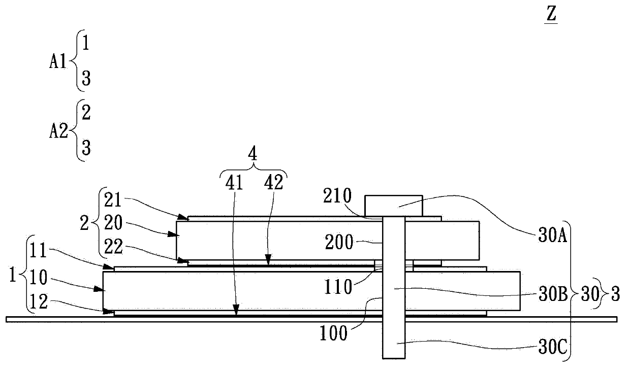
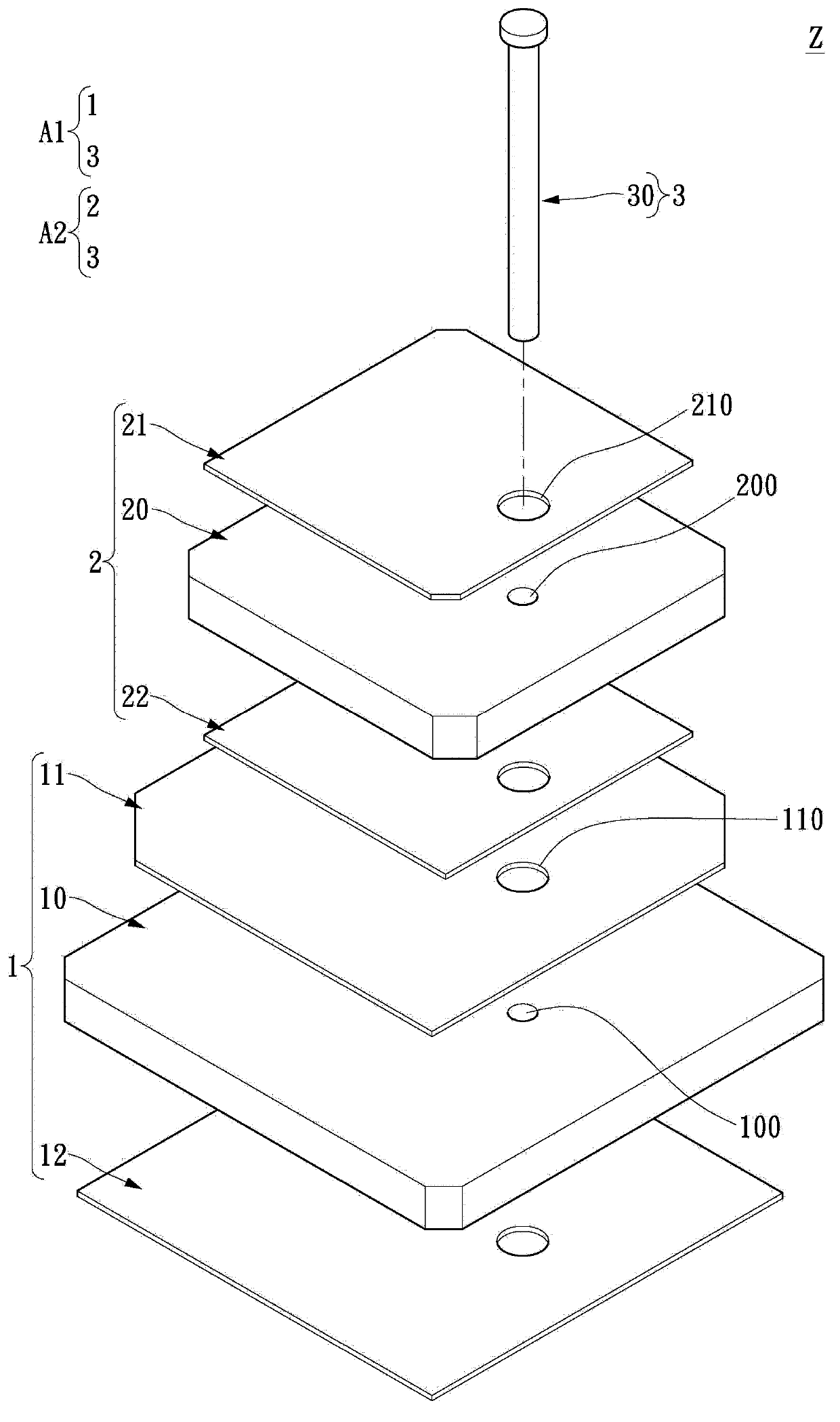
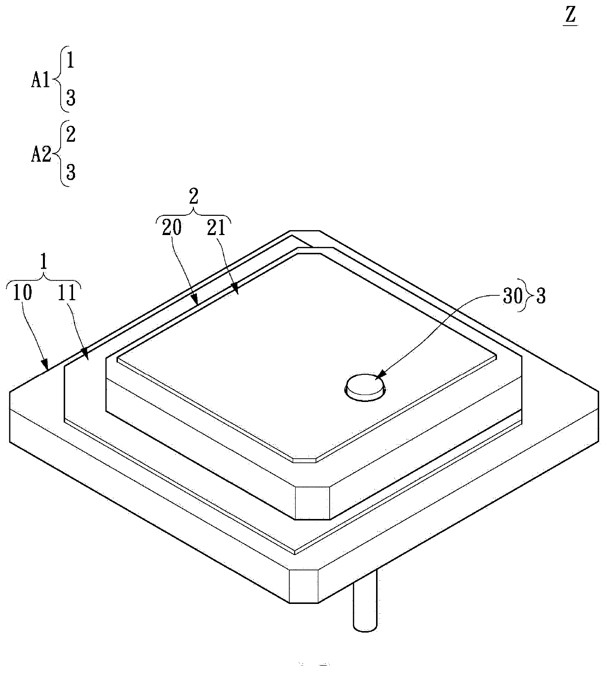
[0047] see figure 1 As shown, the first embodiment of the present invention provides a dual-band antenna structure Z, which includes: a first substrate unit 1 , a second substrate unit 2 and a pin unit 3 . In the first embodiment, at least one feed pin 30 passes through the first electrode through hole 110 and is insulated from the first electrode layer 11 , and the feed pin 30 passes through the second electrode through hole 210 and contacts the second electrode layer 21 , and the first set working frequency band of the first antenna A1 is greater than the second set working frequency band of the second antenna A2. Furthermore, when the first set working frequency band of the first antenna A1 is greater than the second set working frequency band of the second antenna A2, the feeding pin 30 passes through the first electrode through hole 110 and connects with the first electrode layer 11 They are insulated from each other, and the feeding pins 30 pass through the second elect...

no. 2 example

[0049] see Figure 2 to Figure 5 As shown, the second embodiment of the present invention provides a dual-band antenna structure Z, which includes: a first substrate unit 1 , a second substrate unit 2 and a pin unit 3 .

[0050] First, the first substrate unit 1 includes a first insulating substrate 10 and a first electrode layer 11 disposed on the top of the first insulating substrate 10, wherein the bottom of the first insulating substrate 10 has a first ground layer 12, The first insulating substrate 10 has a first through-substrate hole 100 , and the first electrode layer 11 has a first electrode through-substrate hole 110 corresponding to the first through-substrate hole 100 and larger than the first through-substrate hole 100 . In addition, the first insulating substrate 10 has a first dielectric constant. For example, the first insulating substrate 10 can be a ceramic substrate, and the first electrode layer 11 can be a conductive layer made of any conductive material....


PUM


Abstract

The invention relates to a dual-frequency band antenna structure and a manufacturing method thereof. The dual-frequency band antenna structure comprises a first substrate unit, a second substrate unit, and an adhesion unit. The first substrate unit consists of a first insulating substrate, a first electrode layer and a first ground layer; the second substrate unit includes a second insulating substrate, a second electrode layer and a second ground layer, wherein a second dielectric coefficient is larger than a first dielectric coefficient; and a connecting pin unit includes a feed connecting pin successively penetrating the second substrate unit and the first substrate unit, wherein the feed connecting pin is insulated with the first electrode layer and the second electrode layer mutually and the first ground layer and the second ground layer are insulated with each other. The first substrate unit and the connecting pin unit cooperate with each other to form a first antenna with a first set working frequency band; and the second substrate unit and the connecting pin unit cooperate with each other to form a second antenna with a second set working frequency band, wherein the first set working frequency band is larger than the second set working frequency band.

Description

technical field [0001] The invention relates to an antenna structure and a manufacturing method thereof, in particular to a dual-band antenna structure and a manufacturing method thereof. Background technique [0002] With the development of communication technology, various electronic products using wireless communication technology have been born one after another, such as mobile phones, wireless Internet access devices, personal digital assistants and so on. Consumers' requirements for the performance, appearance design and size of these wireless communication devices are also increasing. Taking mobile phones as an example, the receiving frequency has developed from single-band and dual-band to triple-band and quad-band. The appearance of the mobile phone is streamlined and novel, and at the same time it has the characteristics of small size, light weight, and portability. Furthermore, due to the advancement of communication technology, an antenna with dual-frequency and...

Claims


Application Information

Patent Timeline
IPC IPC(8): H01Q21/30H01Q1/38H01Q1/50
Inventor 林俊佑郑大福苏志铭
Owner INPAQ TECH
Why Eureka
Try Eureka