Hybrid infrared detector array and CMOS readout integrated circuit with improved dynamic range

a detector array and integrated circuit technology, applied in the field of solid-state electronic image sensors, can solve the problems of high volume commercial grade cmos imaging products, sensor characteristics close to those of ccd, and high cost and complexity of silicon ccd manufacturing processes, and achieve low dynamic range, high signal-to-noise ratio, and high gain

Active Publication Date: 2009-06-23
THE BF GOODRICH CO
View PDF13 Cites 100 Cited by
  • Summary
  • Abstract
  • Description
  • Claims
  • Application Information

AI Technical Summary

Benefits of technology

[0049]d) a second relatively higher gain, lower dynamic range amplifier circuit responsive to signal received at the second detector input node, the second circuit optimized to provide a high signal to noise ratio for low light level input signals;

Problems solved by technology

The processes related to silicon CCD manufacturing have always been reasonably expensive and complex, with the implementation technology of choice being N type metal oxide (NMOS).
Today, CMOS imager development has yielded a sensor with characteristics close to that of the CCD, but still lacking in some respects.
Few, if any, high volume commercial grade CMOS imaging products are manufactured using uniquely customized image sensor specific processes or complex pixel design technologies.
Although some CMOS imager foundries have begun to support unique process modifications to create specific process and design features for application specific integrated circuit (ASIC) clients, in nearly every case the custom CMOS image sensor technologies that enable these high performance applications are unique to the ASIC client, and not accessible to other users.
However, as airborne reconnaissance systems begin to incorporate additional functionality and interoperability through reductions in size, weight, power, and cost, it is becoming increasingly difficult for CCD technology to support these objectives, due to limitations in the fundamental fabrication and operational principles of the CCD image sensor itself.
Although present CMOS image sensor technology does not support the broad, demanding performance requirements currently provided by the CCD, the successful evolution of airborne reconnaissance imaging systems will rely on the adaptation of CMOS image sensor technology to enable the improvements necessary to advance the art.
The prior art methods to extend detector dynamic range do not preserve the linear response of the detector while maintaining signal integrity for both high and low scene illumination levels.
The full well capacity of a CCD image sensor pixel is generally limited by the charge handling capacity of a gated potential well that usually has an antiblooming feature to avoid signal charge from mixing with adjacent pixels when a pixel that has reached its well saturation limit.
Conversely, the saturation limit of a CMOS image sensor is typically more a complex function of the floating diffusion sense node voltage swing, photodiode storage capacity, and additional capacitances added to the pixel amplifier circuit.
Unfortunately, the maximum voltage swing is limited by the maximum allowable Vdd voltage for the CMOS process design rules being used.
As previously stated, this creates a conflict for conventional pixel design.

Method used


Image

  • Hybrid infrared detector array and CMOS readout integrated circuit with improved dynamic range
  • Hybrid infrared detector array and CMOS readout integrated circuit with improved dynamic range
  • Hybrid infrared detector array and CMOS readout integrated circuit with improved dynamic range

Examples


Embodiment Construction

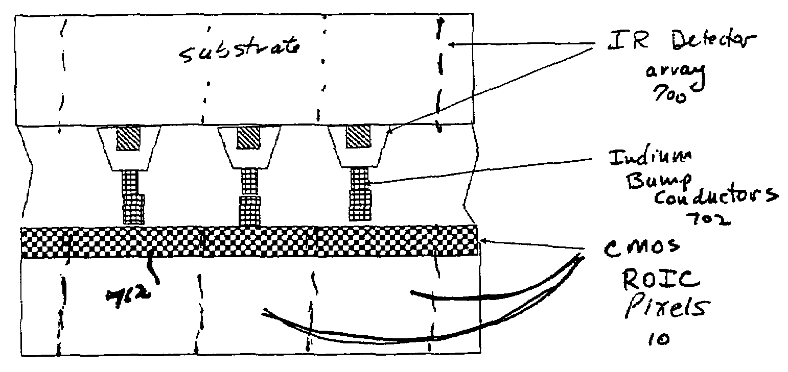
[0083]Before describing hybrid infrared detector array embodiments, a description is set forth of presently preferred CMOS imaging arrays which are suitable for the CMOS dual amplifier readout integrated circuit portion of a hybrid detector array. The inventive methods and devices are applicable to other CMOS imaging array designs and the following descriptions are offered by way of illustration and not limitation. A disclosure of methods for detecting moving objects in a scene is also provided which can be used with the hybrid infrared detector array.

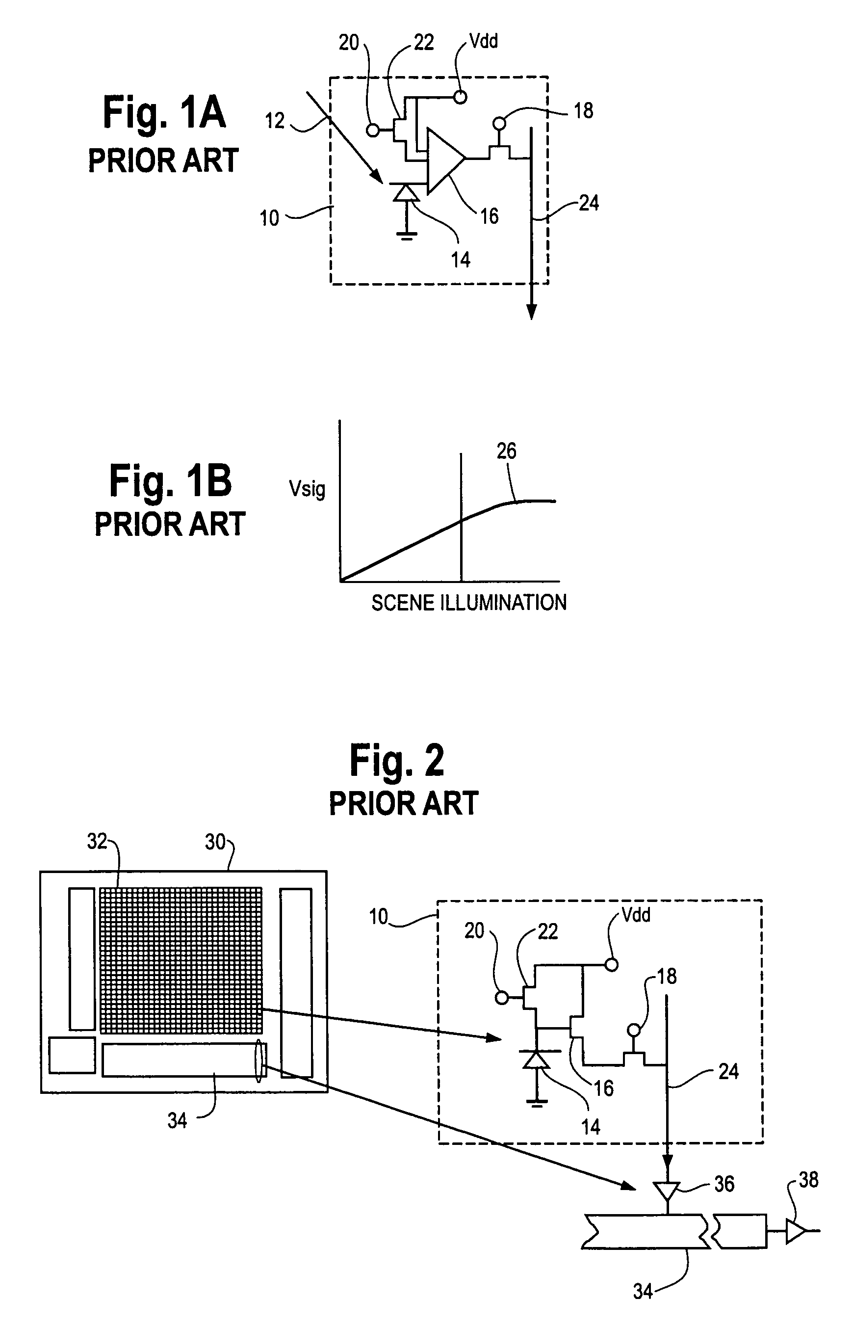
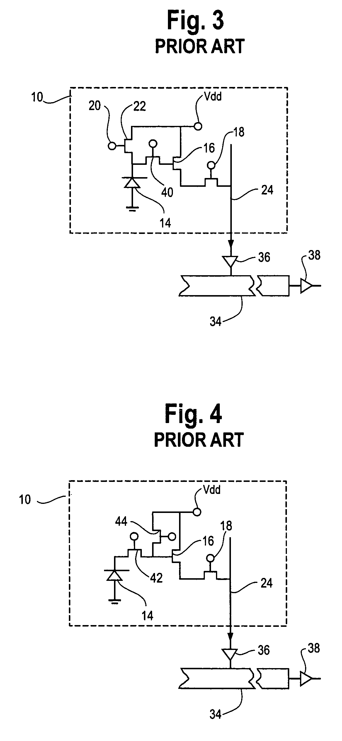
[0084]An improved CMOS imaging array is described below comprising a plurality of individual pixels arranged in an array of rows and columns of individual pixels. The number of pixels can vary, but embodiments of 25 and 50 million pixels are considered exemplary. Each pixel in the plurality of individual pixel sensors is preferably the same. A representative example of the CMOS pixel sensor 10 is shown in FIG. 5A. In this embodiment, t...


PUM


Abstract

A hybrid image sensor includes an infrared detector array and a CMOS readout integrated circuit (ROIC). The CMOS ROIC is coupled to at least one detector of the IR detector array, e.g., via indium bump bonding. Each pixel of the CMOS ROIC includes a first, relatively lower gain, wide dynamic range amplifier circuit which is optimized for a linear response to high light level input signals from the IR detector. Each pixel also includes a second, relatively higher gain, lower dynamic range amplifier circuit which is optimized to provide a high signal to noise ratio for low light level input signals from the IR detector (or from a second IR detector). A first output select circuit is provided for directing the output of the first circuit to a first output multiplexer. A second output select circuit is provided for directing the output of the second circuit to a second output multiplexer. Thus, separate outputs of the first and second circuits are provided for each of the individual pixel sensors of the CMOS imaging array.

Description

CROSS-REFERENCE TO RELATED APPLICATION[0001]This is a continuation-in-part of prior U.S. application Ser. No. 11 / 030,843 filed Jan. 6, 2005, pending, the entire contents of which is incorporated by reference herein. Priority is hereby claimed to the '843 application.BACKGROUND OF THE INVENTION[0002]A. Field of the Invention[0003]The present invention relates to solid state electronic image sensors and in particular to an Infra-Red (IR) focal plane readout integrated circuit. It is particularly suitable for application to airborne imaging systems, such as military aerial reconnaissance and surveillance image sensors.[0004]B. Description of Related Art[0005]Image sensors for capturing electronic representations of images in the visible wavelengths have been around since about 1970, when the silicon charge coupled device (CCD) was invented. Over the years, CCDs have become the standard for visible spectrum electronic imaging, replacing film in most applications. Various architectures h...

Claims


Application Information

Patent Timeline
Patent Type & Authority Patents(United States)
IPC IPC(8): H04N3/14H01L27/00H04N5/335H04N5/33H04N5/355H04N5/357H04N5/3745
CPCH01L27/14603H01L27/14609H01L27/14634H01L27/14659H04N5/33H04N5/35545H04N5/35563H04N5/3559H04N5/3745H01L27/14621H01L27/14632H04N5/374H04N25/581H04N25/585H04N25/59H04N25/76H04N25/77
Inventor FARRIER, MICHAEL
Owner THE BF GOODRICH CO
Why Eureka
Try Eureka