Check patentability & draft patents in minutes with Patsnap Eureka AI!

PCB test fixture

A technology for testing fixtures and PCB boards, which is applied in the direction of electronic circuit testing, measuring device casings, etc., can solve problems such as inability to test or test accuracy, increase cost, and narrow application range, achieve good application prospects, increase replacement speed, reduce The effect of production costs

Inactive Publication Date: 2014-08-27
SUZHOU KUEN ELECTRONICS TECH
View PDF8 Cites 15 Cited by
  • Summary
  • Abstract
  • Description
  • Claims
  • Application Information

AI Technical Summary

Problems solved by technology

The current PCB board inspection fixture does not have a good positioning system. After the pressure plate drives the probe down, the probe may not be aligned with the test point, resulting in low detection accuracy and unable to meet the detection needs.
At the same time, the PCB board is prone to shaking during detection. Generally, an L-shaped baffle is used to fix the PCB board. However, when the PCB board area is large, it is often not fixed firmly, and the length of the baffle board needs to be increased. When the PCB board area is small , too long baffle will also have a certain impact on the detection, the practicability is poor, and the scope of application is narrow, which leads to the inconvenience of PCB board detection, slow welding speed and low precision
[0003] At the same time, pinholes are directly set on the needle plate at present, so that the probe can be directly inserted into the pinhole for subsequent detection. However, if the probe is damaged, it must exit the pinhole. Since the cross-sectional area of ​​each part of the probe is different, After exiting, the diameter of the pinhole will become larger. After the probe is placed again, due to the larger hole diameter, the probe will be tilted after the PCB board is pressed against the probe again, which will cause the probe to not touch the test point, resulting in failure. The test or test accuracy is greatly reduced, which affects the use of the equipment, and the needle board must be replaced with a new needle board, which greatly increases the cost. At the same time, the current needle board has detailed requirements for the design of the pinhole and the length of the probe inserted into the pinhole. , each needle board can only be used for the detection of one product, the versatility is poor, and the scope of application is small

Method used


Image

  • PCB test fixture
  • PCB test fixture
  • PCB test fixture

Examples


Embodiment Construction

[0017] The present invention will be further described below in conjunction with the accompanying drawings.

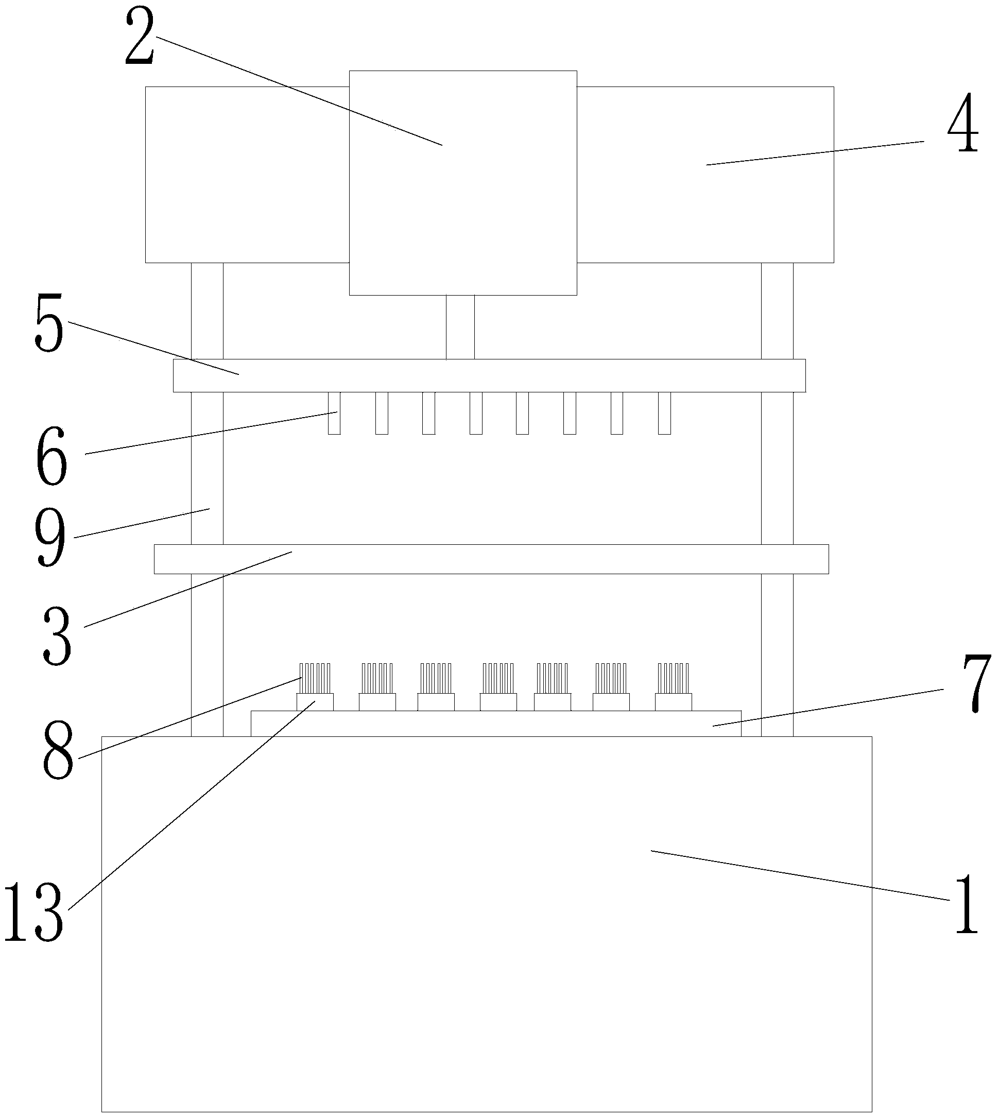
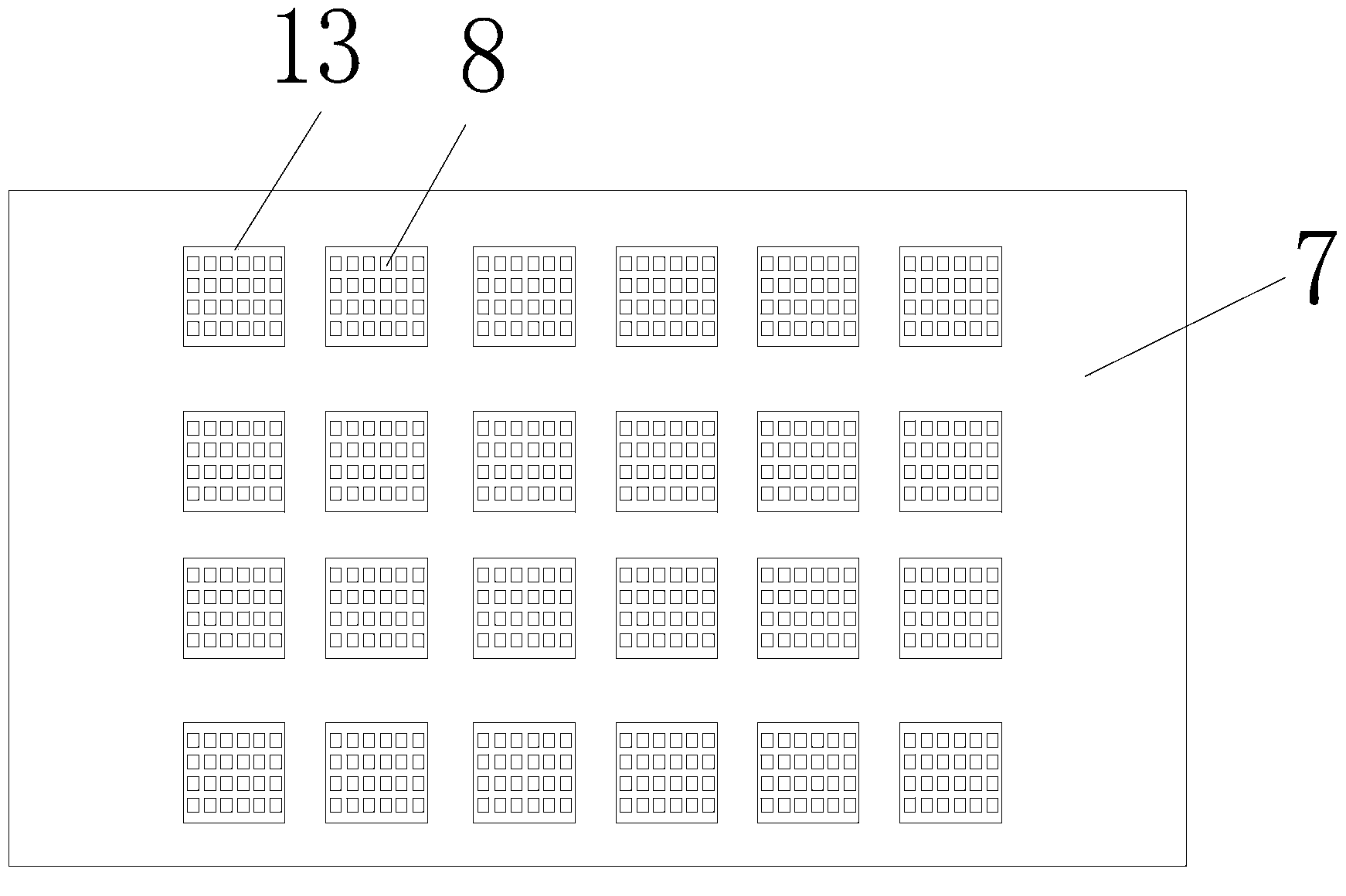
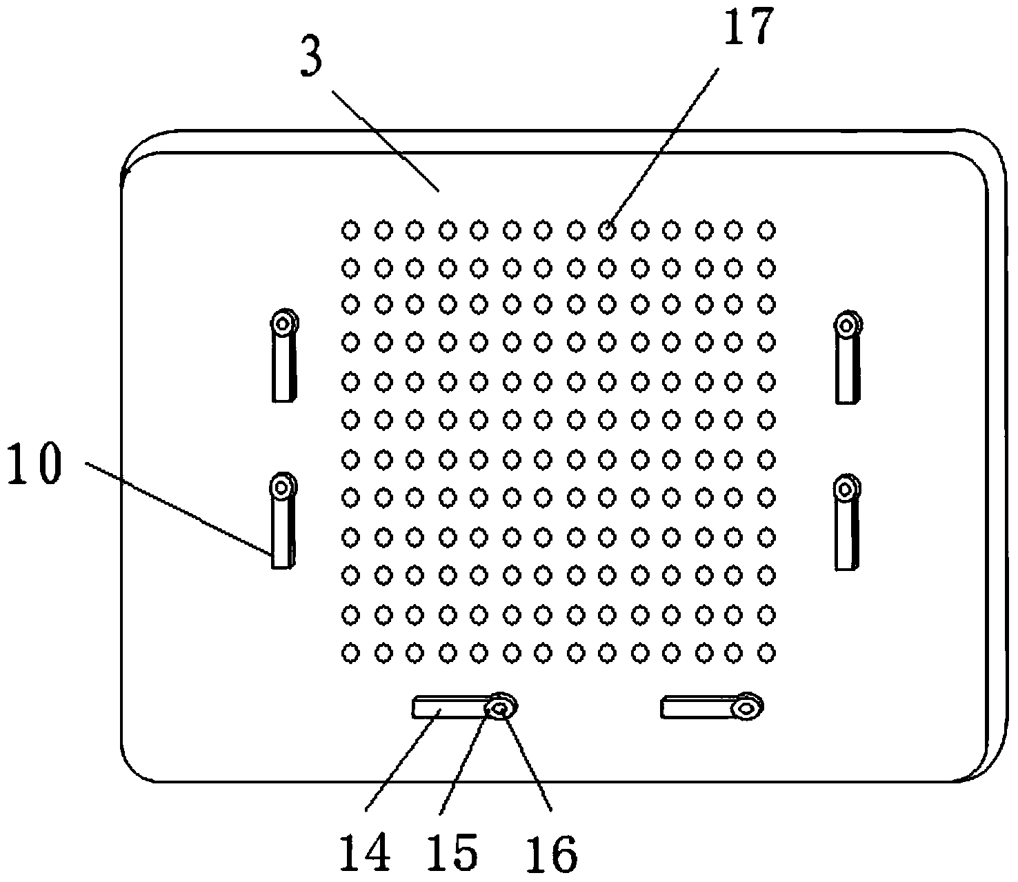
[0018] Such as Figure 1-3 As shown, a PCB board test fixture includes a test bench 1, a cylinder 2, a carrier plate 3, a top plate 4, a pressure plate 5, an upper probe 6, a lower needle plate 7, a lower probe 8, a guide rail 9 and a rotating baffle 10. A top plate 4 is set above the test bench 1, a guide rail 9 is set between the top plate 4 and the test bench 1, a cylinder 2 is set on the front surface of the top plate 4, and a pressure plate 5 is connected to the bottom of the cylinder rod of the cylinder 2, so The pressure plate 5 passes through the guide rail 9 and can slide up and down along the guide rail 9. A number of upper probes 6 are arranged at the bottom of the pressure plate 5, and a carrier plate 3 that can slide along the guide rail 9 is provided below the pressure plate 5. The pressure plate 5 The width is smaller than the width of the carrier board...


PUM


Abstract

The invention discloses a PCB test fixture. The PCB test fixture comprises a test board and a cylinder. The PCB test fixture is characterized in that a top plate is arranged above the test board, a guide rail is arranged between the top plate and the test board, the cylinder is arranged on the front surface of the top plate, a pressing plate is connected to the bottom of a cylinder rod of the cylinder, the pressing plate penetrates through the guide rail, upper probes are arranged on the bottom of the pressing plate, a carrying plate is arranged below the pressing plate, rotary baffles are arranged on the top of the carrying plate, each rotary baffle comprises a stop strip, a movable shaft sleeve and a positioning shaft, each stop strip is connected to the corresponding positioning shaft through the corresponding movable shaft sleeve in a sleeved mode, a plurality of probe holes allowing lower probes to penetrate through are formed in the carrying plate, the lower probes are arranged on the top of the test board, a plurality of positioning holes are formed in a lower probe plate, probe blocks are detachably installed in the positioning holes, the lower probes are arranged on the probe blocks, and springs are arranged between the lower probes and the carrying plate. The PCB test fixture is simple in structure, high in detection precision, high in university and long in service life.

Description

technical field [0001] The invention relates to a testing jig, in particular to a PCB board testing jig. Background technique [0002] The Chinese name of PCB board is printed circuit board, also known as printed circuit board and printed circuit board. It is an important electronic component, a support for electronic components, and a provider of electrical connections for electronic components. Because it is made using electronic printing, it is called a "printed" circuit board. The current PCB board inspection fixture does not have a good positioning system. After the pressure plate drives the probe down, the probe may not be aligned with the test point, resulting in low detection accuracy and unable to meet the detection needs. At the same time, the PCB board is prone to shaking during detection. Generally, an L-shaped baffle is used to fix the PCB board. However, when the PCB board area is large, it is often not fixed firmly, and the length of the baffle board needs to...

Claims


Application Information

Patent Timeline
Patent Type & Authority Applications(China)
IPC IPC(8): G01R31/28G01R1/04
Inventor 杨俊民
Owner SUZHOU KUEN ELECTRONICS TECH
Features
  • R&D
  • Intellectual Property
  • Life Sciences
  • Materials
  • Tech Scout
  • Unparalleled Data Quality
  • Higher Quality Content
  • 60% Fewer Hallucinations
Learn More