Thin-film transistor, array substrate and display device

A technology of thin film transistors and array substrates, applied in the display field, can solve the problems of limited length and rapid increase of off-state current, achieve a large aperture ratio, reduce the occupied area, and improve the effect of rapid increase of off-state current

Inactive Publication Date: 2014-09-03
BOE TECH GRP CO LTD
View PDF6 Cites 23 Cited by
  • Summary
  • Abstract
  • Description
  • Claims
  • Application Information

AI Technical Summary

Problems solved by technology

[0006] Embodiments of the present invention provide a thin film transistor, an array substrate, and a display device, which are used to solve the short-term off-s

Method used


Image

  • Thin-film transistor, array substrate and display device
  • Thin-film transistor, array substrate and display device
  • Thin-film transistor, array substrate and display device

Examples


Example Embodiment

[0028] The specific implementations of the thin film transistor, the array substrate and the display device provided by the embodiments of the present invention will be described in detail below with reference to the accompanying drawings.

[0029] The thickness of each film layer and the size and shape of the area in the drawings do not reflect the true proportions of the components of the thin film transistor, and the purpose is only to schematically illustrate the content of the present invention.
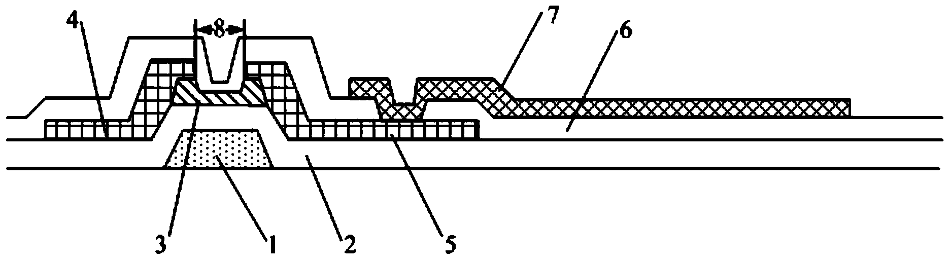
[0030] An embodiment of the present invention provides a thin film transistor, such as image 3 As shown, it includes: a gate electrode 01, an active layer 02, a source electrode 03 and a drain electrode 04 located on a base substrate; the source electrode 03 and the drain electrode 04 are opposed to each other and are electrically connected to the active layer 02 respectively;

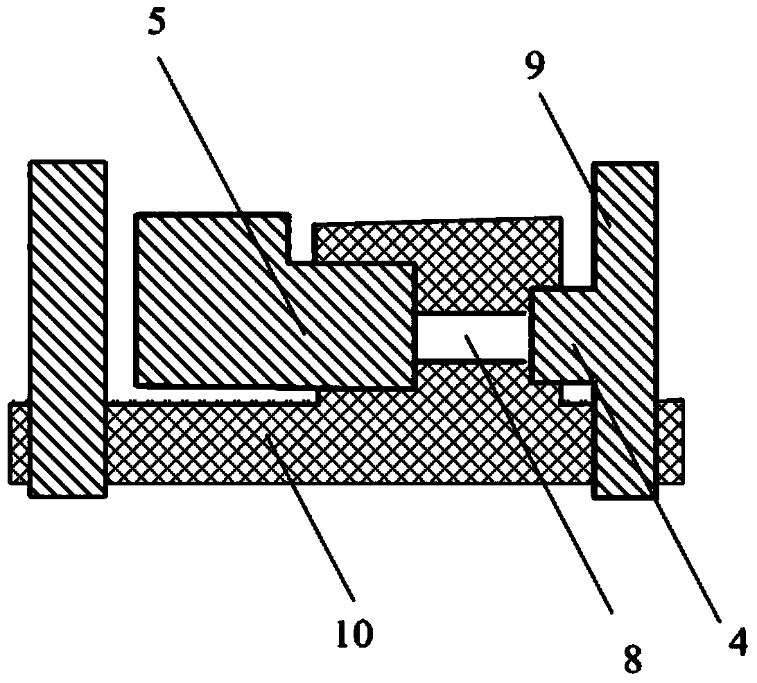
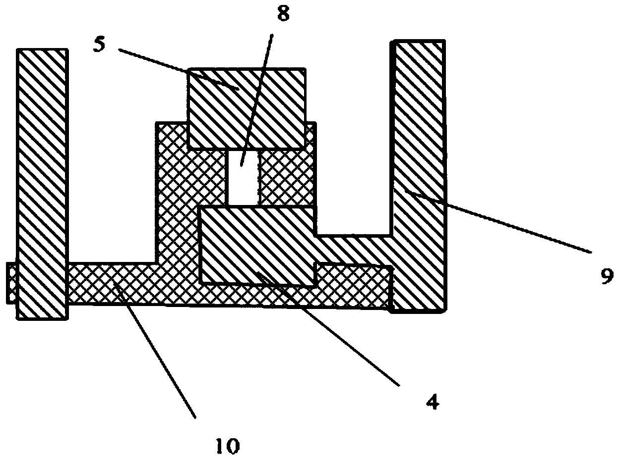
[0031] Such as Figure 4a to Figure 4c As shown, the shape of the orthographic projection of the active laye...


PUM


Abstract

The invention discloses a thin-film transistor, an array substrate and a display device. An active layer area which corresponds with a gap between a source electrode and a drain electrode in the thin-film transistor is designed to a bent shape. Relative to a linear active layer area which corresponds with the gap between the source electrode and the drain electrode in the prior art, the length of the active layer area which corresponds with the gap between the source electrode and the drain electrode increases, thereby settling a problem of off current surge. Furthermore, on condition that the areas of the thin-film transistors are same, the length of the active layer area which corresponds with the gap between the source electrode and the drain electrode increases, thereby reducing the area of the thin-film transistor on condition that the off current is ensured. Particularly, when the thin-film transistor is used for high-resolution display, a relatively large aperture ratio can be ensured.

Description

technical field [0001] The invention relates to the field of display technology, in particular to a thin film transistor, an array substrate and a display device. Background technique [0002] Currently, display devices such as liquid crystal display panels (LCD, Liquid Crystal Display), electroluminescence (EL, electroluminescence) display panels, and electronic paper are well known. These display devices have a thin film transistor (TFT, Thin Film Transistor) that controls the switching of each pixel, and the TFT can be divided into top-gate TFT and bottom-gate TFT according to different structures. [0003] Taking the bottom gate type as an example, thin film transistors such as figure 1 As shown, it consists of a gate 1, an active layer 3, a source 4 and a drain 5 sequentially arranged on the base substrate; wherein, a gate insulating layer 2 is arranged between the gate 1 and the active layer 3, and the source The electrode 4 and the drain electrode 5 are arranged on ...

Claims


Application Information

Patent Timeline
IPC IPC(8): H01L29/786H01L29/06H01L27/02
CPCH01L27/1222H01L29/1037H01L29/78642H01L29/78696G02F1/136286H01L27/1244H01L29/78669H01L29/7869H01L27/1251
Inventor 严允晟王孝林姚星王海燕
Owner BOE TECH GRP CO LTD
Why Eureka
Try Eureka