TFT array substrate, display panel and manufacturing method of display panel

A technology for array substrates and display panels, which is used in semiconductor/solid-state device manufacturing, electrical components, electrical solid-state devices, etc., can solve the problems of increasing manufacturing cost and process complexity, and cannot meet high aperture ratios, and achieves lower manufacturing costs and The complexity of the process, the high aperture ratio, and the effect of satisfying the aperture ratio

Inactive Publication Date: 2014-07-16
KUSN INFOVISION OPTOELECTRONICS
View PDF4 Cites 13 Cited by
  • Summary
  • Abstract
  • Description
  • Claims
  • Application Information

AI Technical Summary

Problems solved by technology

see Figure 1i In the AB region, the traditional TFT array substrate needs to occupy a large area to set the via hole 110', so it cannot meet the requirement of high aperture ratio, and the via hole 110' needs to be formed in two photomask processes, which increases the manufacturing cost and the complexity of the process

Method used


Image

  • TFT array substrate, display panel and manufacturing method of display panel
  • TFT array substrate, display panel and manufacturing method of display panel
  • TFT array substrate, display panel and manufacturing method of display panel

Examples


no. 1 example

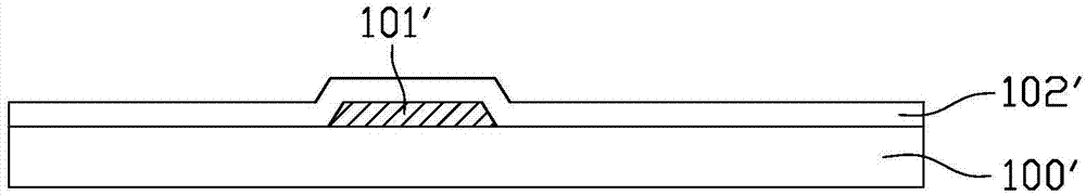
[0042] Figure 2a It is a partial cross-sectional schematic diagram of the TFT array substrate according to the first embodiment of the present invention. Figure 2b It is a partial plan view of the TFT array substrate according to the first embodiment of the present invention. Please also see Figure 2a and Figure 2b The TFT array substrate includes a gate metal layer 101, a gate insulating layer 102, a semiconductor layer 103, a source / drain metal layer 104, a first protective layer 105, a flat layer 106, a pixel electrode 107, The second protective layer 108 and the common electrode 109 . Wherein, the source / drain metal layer 104 includes a source metal layer 1041 and a drain metal layer 1042, the source metal layer 1041 and the drain metal layer 1042 are separated from each other and located in the same layer, and are arranged between the gate metal layer 101 and the semiconductor layer. 103 is in contact with the semiconductor layer 103 , so that a part of the semico...

no. 2 example

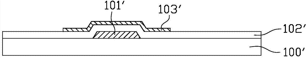
[0068] Figure 4 It is a partial cross-sectional schematic diagram of a TFT array substrate according to the second embodiment of the present invention. Such as Figure 4 The TFT array substrate shown with Figure 2aThe difference of the TFT array substrate shown is that the semiconductor layer 103 is indium gallium zinc oxide (IGZO), and the TFT array substrate further includes an etching stopper layer 203 disposed on the semiconductor layer 103 . Compared with amorphous silicon (a-si), IGZO has the characteristics of high mobility and good uniformity, so it can better realize large-size high-resolution panels. In addition, IGZO also has the characteristic of low leakage current, therefore, IGZO can also reduce power consumption as the semiconductor layer 103 . Simultaneously, because IGZO is more sensitive to water, oxygen, therefore adopt IGZO as semiconductor layer 103, it may be polluted easily and change molecular structure and become conductor or insulator material, ...

no. 3 example

[0072] Figure 8 It is a partial cross-sectional schematic diagram of the TFT array substrate according to the third embodiment of the present invention. The present invention as Figure 8 The TFT array substrate shown with Figure 2a The structure of the TFT array substrate shown is basically the same, the difference is that the via hole 110 formed by etching the first protective layer 105 using the patterned flat layer 106 as a photoresist mask is located at the gate metal layer 101 and the drain electrode. Above the metal layer 1042, so compared with the first and second embodiments, the via hole 110 of this embodiment does not need to be formed in the light-transmitting region of the TFT array substrate, so that the pixel electrode 107 is in contact with the drain metal 1042, so This embodiment further increases the aperture ratio.


PUM


Abstract

The invention discloses a thin film transistor array substrate. The TFT array substrate comprises a gate metal layer, a gate insulating layer, a semiconductor layer, a source / drain metal layer, a planar layer, a first protection layer, a first electrode layer, a second protection layer and a second electrode layer, wherein the first electrode layer comprises pixel electrodes, the second electrode layer comprises public electrodes, communicating holes are formed in the planar layer, and the pixel electrodes make contact with the drain metal layer through the communicating holes. The invention further provides a display panel and a manufacturing method of the display panel. According to the manufacturing method, etching is performed on the first protection layer with the planar layer as a light shielding cover to form the communicating holes penetrating through the first protection layer and the planar layer so that the pixel electrodes can make contact with the drain metal layer through the communicating holes, the occupied area of the communicating holes is reduced, and thus the requirement for a high aperture rate can be met; besides, the communicating holes are only formed in the process of one light cover, and thus the manufacturing cost and the complexity of the technology are reduced.

Description

technical field [0001] The invention relates to the field of display technology, in particular to a thin film transistor array substrate. Background technique [0002] With the development of science and technology, thin and light, power-saving information products have flooded our lives, and displays have played a very important role in it. Whether it is a mobile phone, a personal digital assistant or a notebook computer, etc., display devices are required As a platform for man-machine communication. [0003] Thin Film Transistor (TFT) liquid crystal displays are widely used in the display field due to their advantages of high integration, power saving, low cost, and flexible process, and the TFT array substrate process is the key to the manufacturing process of TFT displays. [0004] Figures 1a-1h It is a schematic cross-sectional view of each step in a conventional manufacturing method of a TFT array substrate. Figure 1i It is a partial plan view of a traditional TFT ...

Claims


Application Information

Patent Timeline
IPC IPC(8): H01L27/12H01L23/528H01L21/84H01L21/768
Inventor 潘新叶戴文君钟德镇
Owner KUSN INFOVISION OPTOELECTRONICS
Why Eureka
Try Eureka