Thin film transistor, manufacturing method thereof and corresponding device

A technology of thin-film transistors and display devices, which is applied in the direction of transistors, semiconductor/solid-state device manufacturing, electric solid-state devices, etc., can solve problems such as limiting the application of high-resolution display panels, and achieve the effect of saving the occupied area

Active Publication Date: 2016-07-13
BOE TECH GRP CO LTD
View PDF3 Cites 13 Cited by
  • Summary
  • Abstract
  • Description
  • Claims
  • Application Information

AI Technical Summary

Problems solved by technology

[0004] The present invention provides a thin film transistor, its manufacturing method and corresponding device, which are used to solve the pr

Method used


Image

  • Thin film transistor, manufacturing method thereof and corresponding device
  • Thin film transistor, manufacturing method thereof and corresponding device
  • Thin film transistor, manufacturing method thereof and corresponding device

Examples


Example Embodiment

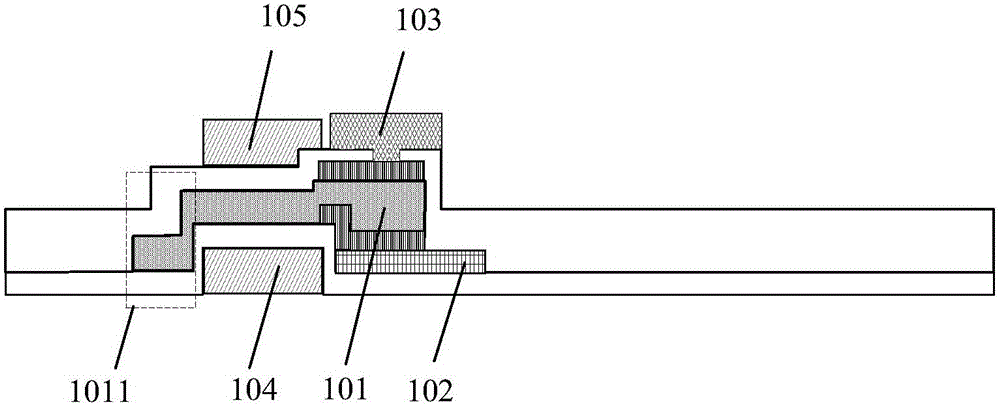
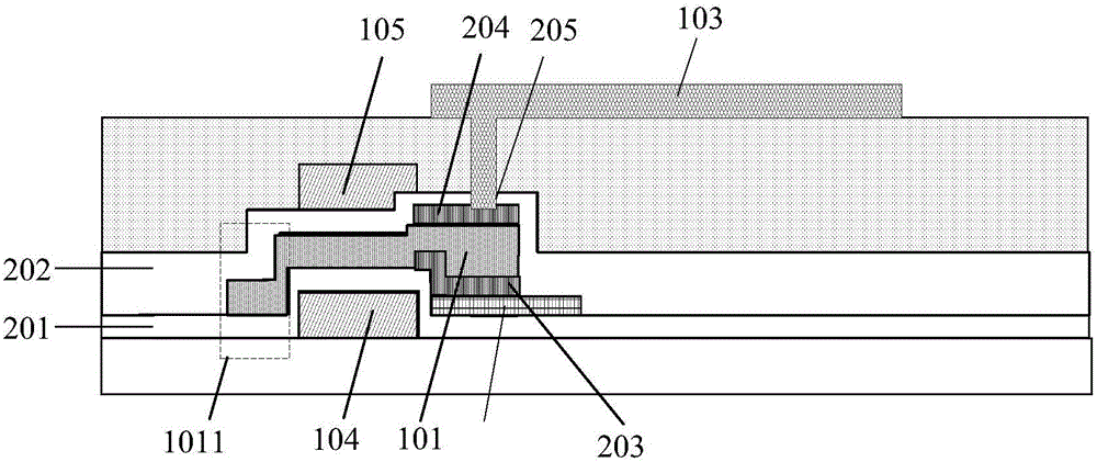
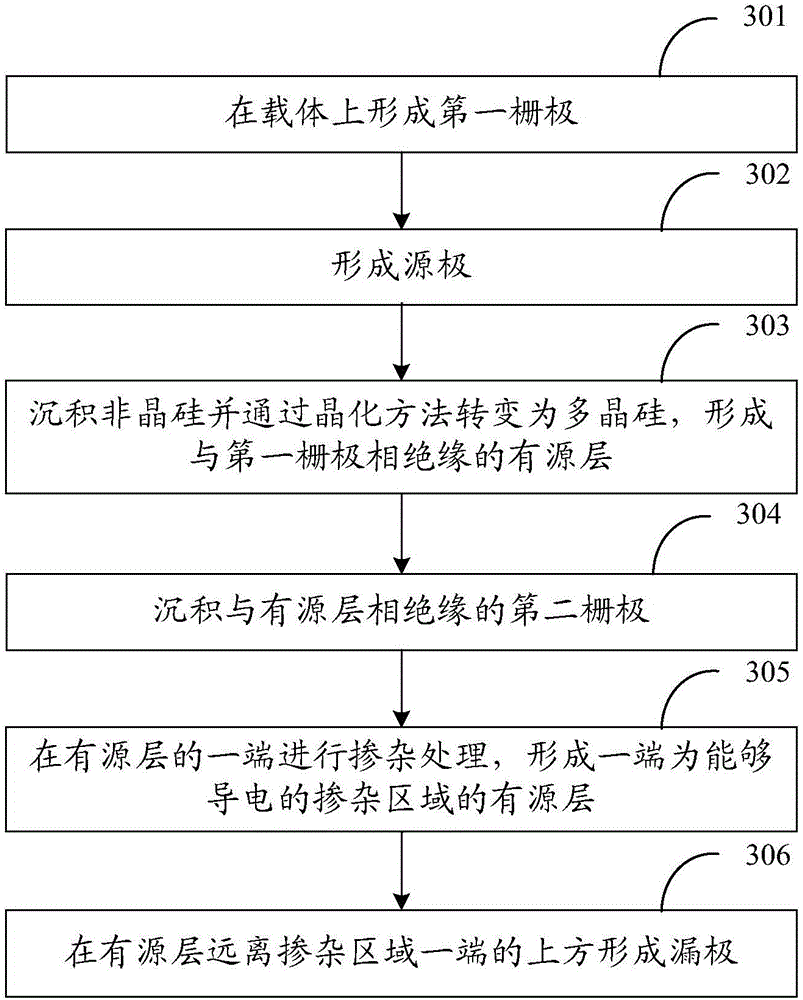
[0038] The thin film transistor provided by the embodiment of the present invention includes: an active layer provided with a conductive doped region at one end; a source and a drain respectively provided below and above the end of the active layer away from the doped region; A first gate and a second gate below and above the source layer and insulated from the active layer. The thin film transistor in the embodiment of the present invention includes two gates respectively distributed on the upper and lower sides of the active layer. Since the channel is formed only on the surface of the active layer, the active layer can be formed on the upper and lower sides during operation. Two layers of channels, and the upper and lower channels are connected through the conductive doped region at one end of the active layer, which occupies a smaller substrate area than the existing structure under the same channel length requirement, which is beneficial to adapt to high resolution The des...


PUM

PropertyMeasurementUnit
Thicknessaaaaaaaaaa

Abstract

The invention relates to a thin film transistor, a manufacturing method thereof and a corresponding device which are used for solving the problem that in a thin film transistor in the prior art, the long channel length limits application of a high resolution display panel. The thin film transistor comprises an active layer, a source, a drain, a first grid and a second grid, wherein one end of the active layer is provided with the active layer is provided with a conductive doping area; the source and the drain are arranged below and above one end of the active layer far away from the doping area respectively; and the first grid and the second grid are arranged below and above the active layer respectively and insulated from the active layer. The thin film transistor comprises the two grids which are distributed on the upper surface and the lower surface of the active layer respectively. Due to the fact that channels only form on the surface of the active layer, the upper layer channel and the lower layer channel can be formed on the upper surface and the lower surface of the active layer in work, the upper channel and the lower channel are connected through the conductive doping area at one end of the active layer, the length of the channels is the sum of the lengths of the channels on the upper surface and the lower surface, and the occupied area is saved better when the same channel length of the current structure is required.

Description

technical field [0001] The invention relates to the technical field of displays, in particular to a thin film transistor, a manufacturing method thereof and a corresponding device. Background technique [0002] At present, compared with amorphous silicon array substrates, low-temperature polysilicon array substrates have the advantages of high mobility (up to hundreds of times the mobility of amorphous silicon array substrates), the size of its thin film transistors can be made small, and the response speed Fast, is an array substrate for display panels that has become more and more popular in recent years, and is increasingly used in high-resolution, high-quality organic electroluminescent displays and liquid crystal display panels. However, its composition is generally complex and the process is numerous. Especially in high-resolution display panels, multiple small-sized thin-film transistors are required, and the requirements for process realization, electrical performanc...

Claims


Application Information

Patent Timeline
IPC IPC(8): H01L29/786H01L29/06H01L21/336H01L27/12H01L27/32
CPCH01L27/1214H01L29/1033H01L29/6675H01L29/78696H10K59/12
Inventor 刘政
Owner BOE TECH GRP CO LTD
Why Eureka
Try Eureka