Flash sense amplifier

A sensitive amplifier and sensitive amplification technology, which is applied in the direction of instruments, static memory, digital memory information, etc., can solve problems such as unresolved impact, circuit power consumption, circuit working state change, etc.

Inactive Publication Date: 2012-07-04
PEKING UNIV
View PDF4 Cites 14 Cited by
  • Summary
  • Abstract
  • Description
  • Claims
  • Application Information

AI Technical Summary

Problems solved by technology

[0004] One disadvantage of this circuit is that any signal change will bring about a change in the working state of the circuit, resulting in circuit power consumption, even in the stage where no read operation is required
Its biggest advantage is that the amplifier tube can avoid the loss of the leakage voltage caused by the tail control tube. The amplifier tube can work between VDD and GND, and the amplified current is larger and the speed is faster; but it does not solve the problem that the bit line is larger The problem of the effect of parasitic capacitance on the amplifier

Method used


Image

  • Flash sense amplifier
  • Flash sense amplifier
  • Flash sense amplifier

Examples


Embodiment 1

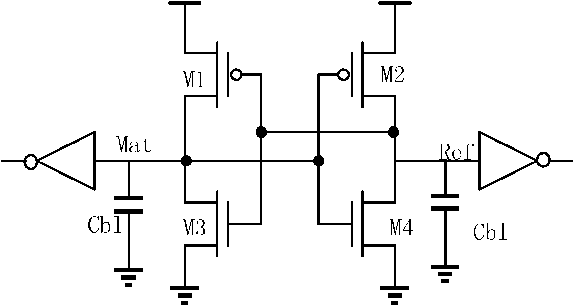
[0047] This embodiment describes a kind of Flash sensitive amplifier, comprising:

[0048] first inverter;

[0049] The second inverter is used to couple with the first inverter to form a bistable circuit of positive feedback amplification;

[0050]The first amplification control unit is used to realize the on-off between the input terminal of the first inverter and the output terminal of the second inverter under the control of the sensitive signal, that is, to connect in the sensitive amplification stage, and in the The potential input stage is disconnected;

[0051] The second amplification control unit is used to realize the on-off between the output terminal of the first inverter and the input terminal of the second inverter under the control of the sensitive signal, that is, in the sensitive amplification stage Connected, disconnected during the potential input stage;

[0052] a third inverter, the input end of which is connected to the input end of the first inverter...

Embodiment 2

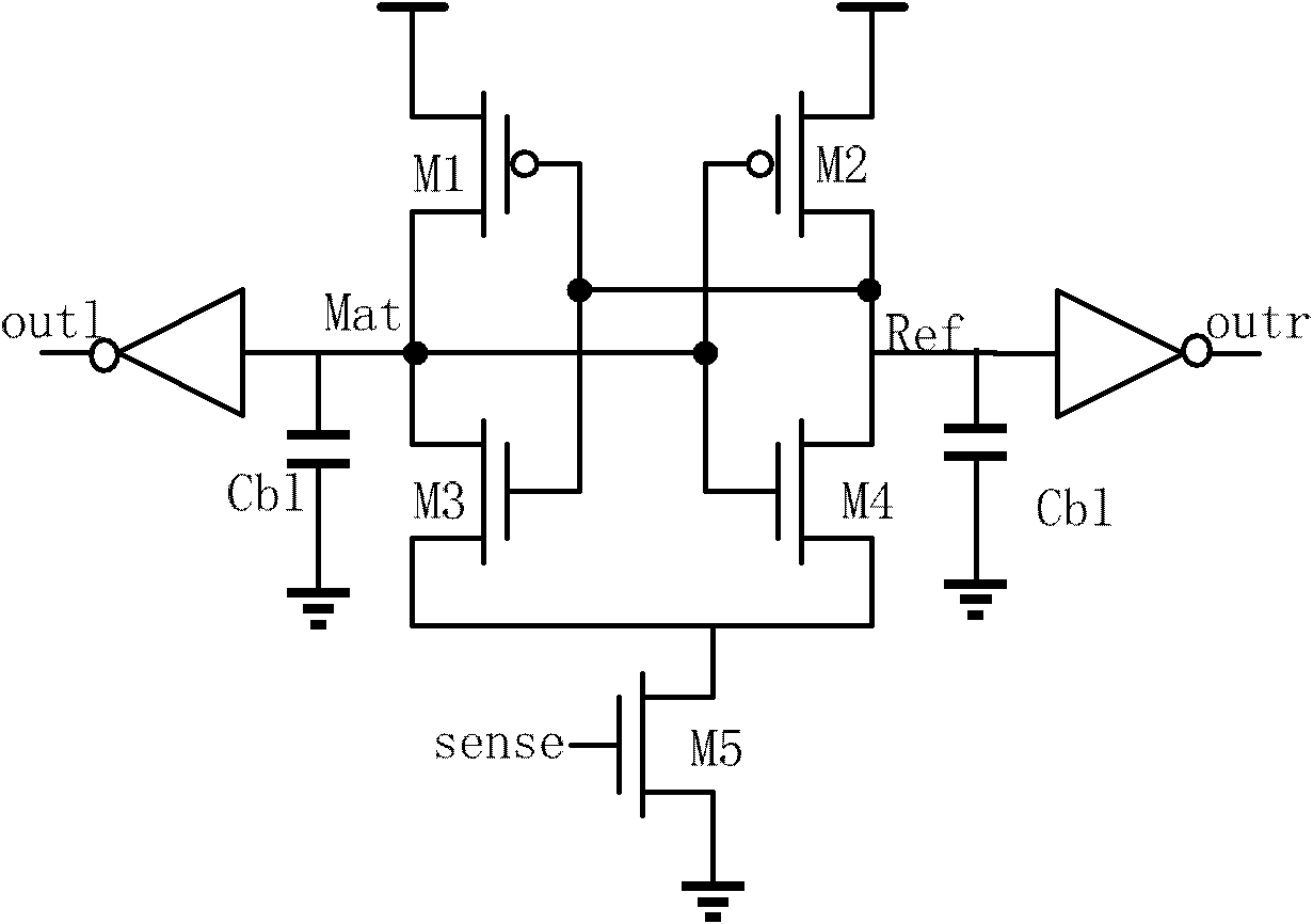
[0061] Such as Figure 5 Shown, the Flash sensitive amplifier of present embodiment record comprises:

[0062] first inverter inv101;

[0063] The second inverter inv102 is used to couple with the first inverter inv101 to form a bistable circuit of positive feedback amplification;

[0064] The gate of the first NMOS transistor M101 is connected to the sensitive signal sense, and the non-gate poles are respectively connected to the input terminal in101 of the first inverter inv101 and the output terminal out102 of the second inverter inv102;

[0065] The gate of the second NMOS transistor M102 is connected to the sensitive signal sense, and the non-gate poles are respectively connected to the output terminal out101 of the first inverter inv101 and the input terminal in102 of the second inverter inv102;

[0066] The third inverter inv103, the input terminal is connected to the input terminal in101 of the first inverter inv101, and the output terminal is connected to the left o...

Embodiment 3

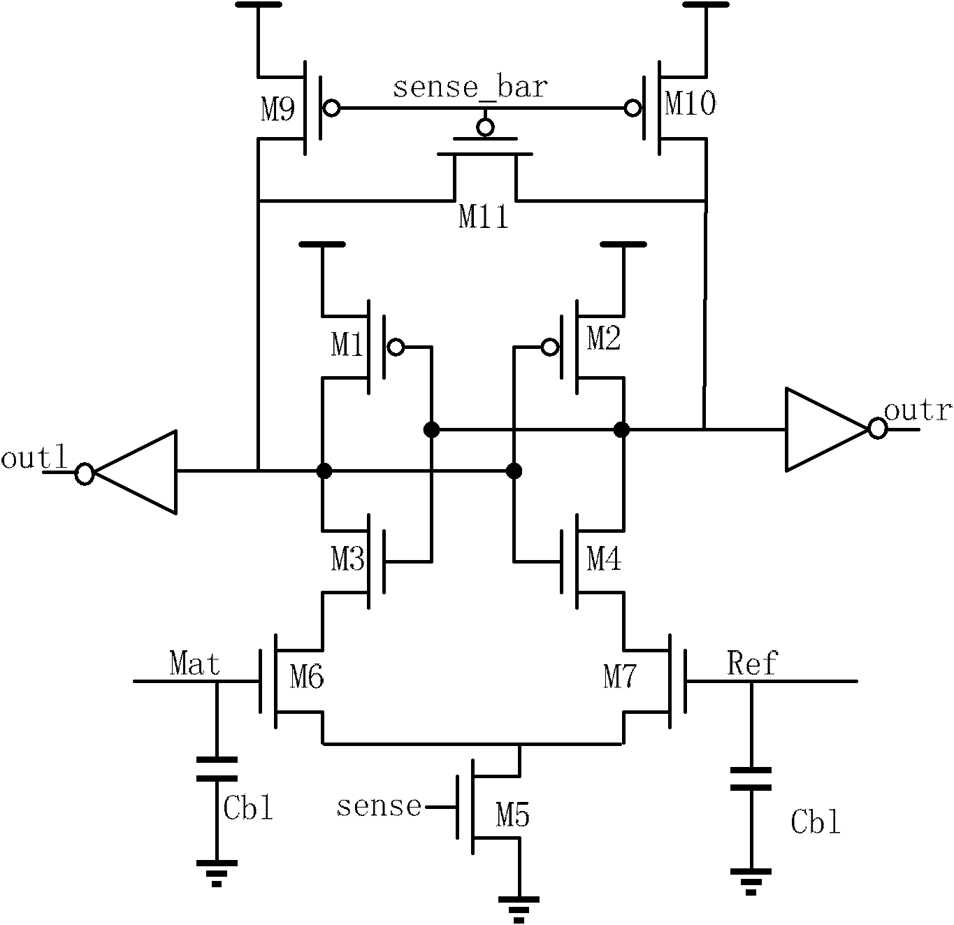
[0084] Such as Figure 8 As shown, the basic structure of this embodiment is the same as that of Embodiment 2, the difference is that this embodiment will:

[0085] The first NMOS transistor in the second embodiment is replaced by the first CMOS transmission gate G201, the gate of the NMOS transistor is connected to the sensitive signal sense, the gate of the PMOS transistor is connected to the dual signal sense_bar complementary to the sensitive signal sense, two The signal input and output terminals are respectively connected to the input terminal in201 of the first inverter inv201 and the output terminal of the second inverter inv202 to out202;

[0086] The second NMOS transistor in the second embodiment is replaced by a second CMOS transmission gate G202, the gate of the NMOS transistor is connected to the sensitive signal sense, the gate of the PMOS transistor is connected to the dual signal sense_bar complementary to the sensitive signal sense, two The signal input and ...


PUM


Abstract

The invention discloses a Flash sense amplifier, which comprises a first inverter, a second inverter, a first amplification control unit, a second amplification control unit, a unit array bit line, a first latch control unit, a reference array bit line and a second latch control unit, wherein the first amplification control unit is used for controlling the make-and-break between an input end of the first inverter and an output end of the second inverter; the second amplification control unit is used for controlling the make-and-break between the output end of the first inverter and the input end of the second inverter; the unit array bit line is used for providing unit bit line potential; the first latch control unit is used for controlling the make-and-break between the unit array bit line and the input end of the first inverter; the reference array bit line is used for providing reference bit line potential; and the second latch control unit is used for controlling the make-and-break between the reference array bit line and the input end of the second inverter. The Flash sense amplifier separates the input of the amplifier from the sense amplification, and reduces the influences of the bit line stray capacitance on the amplifier.

Description

technical field [0001] The invention relates to the technical field of integrated circuits, in particular to a Flash sensitive amplifier. Background technique [0002] Flash is widely used in modern integrated circuits. U disks, digital cameras, and SD cards in smart phones that people are familiar with are all designed based on the Flash structure. Flash performance has become an important direction of IC design. For memory, the speed of reading largely determines the speed of circuit work. With the reduction of the proportionality rules of integrated circuits, the parasitic capacitance on the bit line of a column of memory cells is driven, which becomes the biggest limiting factor in the circuit reading process. The sensitive amplifier is the most important circuit unit structure in the readout channel, and its sensitive amplification speed directly determines the readout speed of the Flash circuit. [0003] Generally common amplifiers use a differential circuit or a c...

Claims


Application Information

Patent Timeline
Patent Type & Authority Applications(China)
IPC IPC(8): G11C7/06
Inventor 王源黄鹏杜刚贾嵩康晋锋张兴
Owner PEKING UNIV
Why Eureka
Try Eureka