Measuring structure and method for Young's modulus of thin film silicon material on insulating substrate

A technology for testing structures on an insulating substrate, applied in the direction of testing the strength of materials by applying a stable bending force, can solve problems such as instability, uncertain device design and performance prediction, and achieve simple test methods, test processes and test results. The effect of stable parameter value and wide adaptability

Inactive Publication Date: 2016-04-13
SOUTHEAST UNIV
View PDF4 Cites 0 Cited by
  • Summary
  • Abstract
  • Description
  • Claims
  • Application Information

AI Technical Summary

Problems solved by technology

[0002] The performance of microelectromechanical devices is closely related to material parameters. Due to the influence of processing, some material parameters will change. These uncertain factors caused by processing technology will make device design and performance prediction uncertain and unstable. Case

Method used


Image

  • Measuring structure and method for Young's modulus of thin film silicon material on insulating substrate
  • Measuring structure and method for Young's modulus of thin film silicon material on insulating substrate
  • Measuring structure and method for Young's modulus of thin film silicon material on insulating substrate

Examples


Embodiment Construction

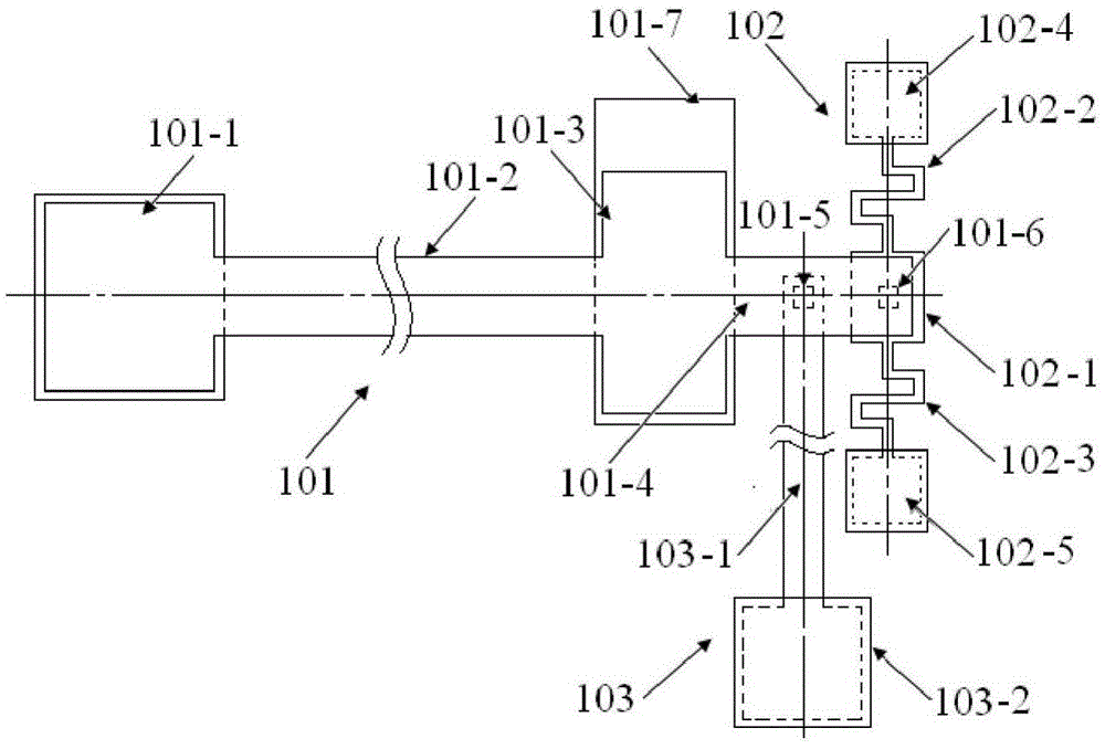
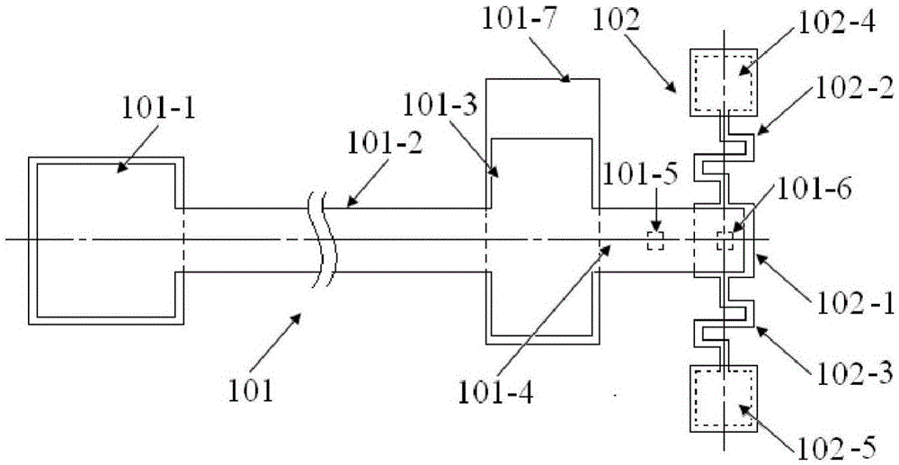
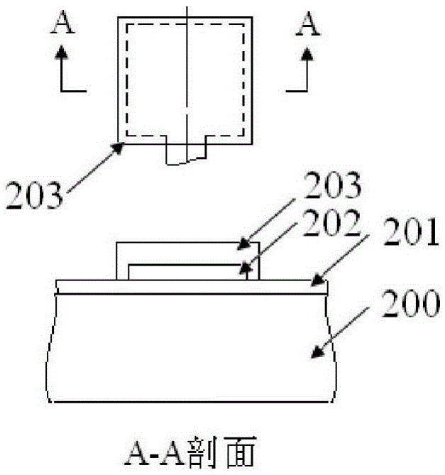
[0031] Attached below figure 1 , figure 2 and image 3 The present invention will be further described.

[0032] The invention provides a test structure for measuring Young's modulus of thin film silicon material on an insulating substrate. The test structure consists of two sets of structures. The first set of structures such as figure 1 As shown, this group of structures consists of a polysilicon cantilever beam 101, a thin-film silicon cantilever beam 103, and a backing plate 102 made of thin-film silicon; the second group is as figure 2 As shown, it consists of a polysilicon cantilever beam 101 and a backing plate 102 made of thin film silicon. The difference between the two groups of structures is whether or not the thin-film silicon cantilever beam 103 is included, and other corresponding unit structures and geometric dimensions in the two groups of structures are identical.

[0033] The polysilicon cantilever beam 101 of the first group of test structures consis...


PUM


Abstract

The invention provides a structure and a method for testing Young modulus of a thin film silicon material on an insulating substrate. The structure comprises two groups of structures, wherein the first group of structures consists of a polycrystalline silicon cantilever beam (101), a thin film silicon cantilever beam (103) and a cushion plate (102) made from polycrystalline silicon; the second group of structures consists of a polycrystalline silicon cantilever beam and a cushion plate made from the polycrystalline silicon. According to the structure, units for actually testing the Young modulus of thin film silicon are the thin film silicon cantilever beams, the only difference of the two groups of structures is whether the thin film silicon cantilever beam exists, and corresponding structures and geometric dimensions of other units in the two groups of structures are completely the same. According to the method, by applying an electrostatic force, the polycrystalline silicon cantilever beams are bent downwards to press the thin film silicon cantilever beam and the cushion plates to contact with the substrate; by testing with the two groups of test structures, a force for independently driving the thin film silicon cantilever beam to be bent to reach test deflection is extracted, and the Young modulus of the thin film silicon material on the insulating substrate can be calculated by virtue of the force, the test deflection and the geometric dimensions.

Description

technical field [0001] The invention provides a testing structure for Young's modulus of thin film silicon material on an insulating substrate. The invention belongs to the technical field of microelectromechanical system (MEMS) material parameter testing. technical background [0002] The performance of microelectromechanical devices is closely related to material parameters. Due to the influence of processing, some material parameters will change. These uncertain factors caused by processing technology will make device design and performance prediction uncertain and unstable. Case. The purpose of material parameter testing is to be able to measure the material parameters of MEMS devices manufactured by a specific process in real time, monitor the stability of the process, and feed back the parameters to the designer so that the design can be corrected. Therefore, testing without leaving the processing environment and using general-purpose equipment has become a necessary...

Claims


Application Information

Patent Timeline
Patent Type & Authority Patents(China)
IPC IPC(8): G01N3/20
Inventor 李伟华王雷张璐周再发
Owner SOUTHEAST UNIV
Why Eureka
Try Eureka