


Quick Research
Generate reliable direction feasibility study reports for your R&D in just a few steps.

Technical Q&A
Discover and master advanced knowledge NOW. Basics, ideas, possibilities, all at once.

Find Solutions
As an expert in R&D theories, this can generate solutions to your technical problems instantly.

Evaluate Feasibility
Analyze your overall solution with one click, know your potential R&D risks in advance.

Monitor Landscape
Get weekly tech updates, stay abreast of the latest tech innovations and key insights.
Display Device
A display device and display area technology, applied in optics, instruments, nonlinear optics, etc., can solve problems such as image defects and improper bonding of substrates to each other, and achieve the effect of simplifying the manufacturing process
- Summary
- Abstract
- Description
- Claims
- Application Information
AI Technical Summary
Problems solved by technology
Method used
Image

Examples
Embodiment Construction
[0028] It will be understood that when an element or layer is referred to as being "on," "connected to" or "coupled to" another element or layer, it can be directly on, Directly connected or bonded to another element or layer, or intervening elements or layers may be present. Throughout, the same reference numerals refer to the same elements.
[0029] Hereinafter, exemplary embodiments of the present disclosure will be described in detail with reference to the accompanying drawings.
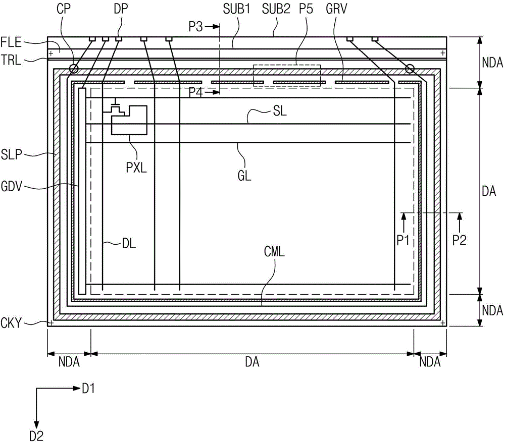
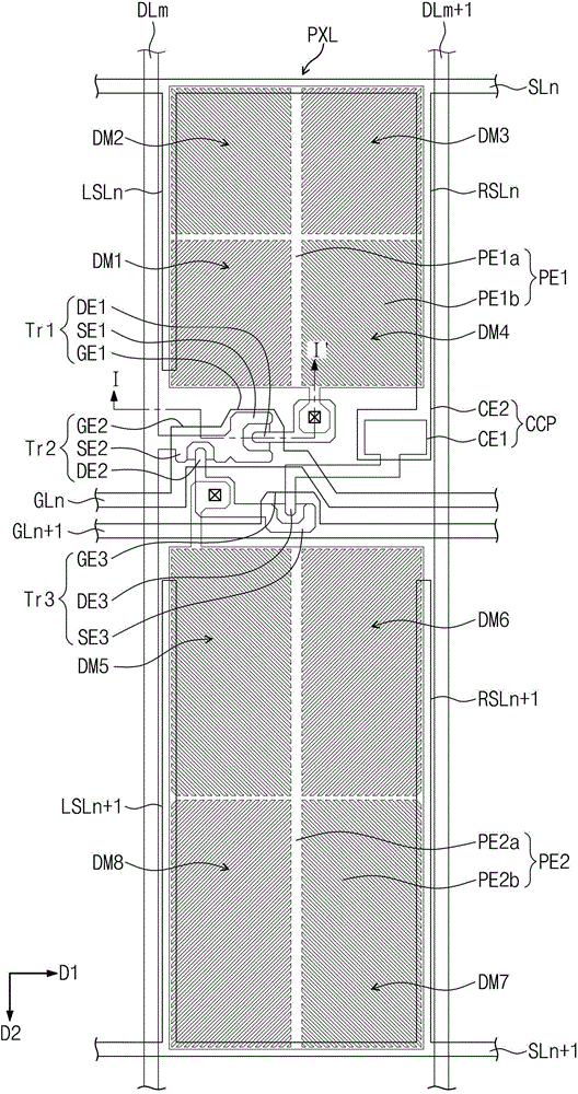
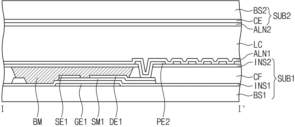
[0030] figure 1 is a plan view of a display device according to an exemplary embodiment of the present disclosure, figure 2 is in figure 1 A plan view of one pixel of the display device shown in, image 3 is along figure 2 A cross-sectional view taken along line II', Figure 4 Yes figure 2 The equivalent circuit diagram of the pixel shown in .
[0031] refer to Figure 1 to Figure 4 , the display device has a rectangular shape including a pair of long sides and a pair of short sides. ...
PUM
 Abstract
Description
Claims
Application Information
 - R&D Engineer
- R&D Manager
- IP Professional
- Industry Leading Data Capabilities
- Powerful AI technology
- Patent DNA Extraction
Browse by: Latest US Patents, China's latest patents, Technical Efficacy Thesaurus, Application Domain, Technology Topic, Popular Technical Reports.
© 2024 PatSnap. All rights reserved.Legal|Privacy policy|Modern Slavery Act Transparency Statement|Sitemap|About US| Contact US: help@patsnap.com