Flip-chip bonding device and bonding method thereof

A flip-chip and bonding device technology, which is applied in the manufacturing of electrical components, electrical solid-state devices, semiconductor/solid-state devices, etc., can solve the problem of reducing the reliability and accuracy of the bonding process, and the inability to accurately obtain semiconductor chips and transfer positions. Accuracy reduction and other issues, to achieve the effect of increasing UPH, reducing thermal expansion and vibration, and reducing movement

Active Publication Date: 2018-02-02
HANMI SEMICON CO LTD
View PDF5 Cites 0 Cited by
  • Summary
  • Abstract
  • Description
  • Claims
  • Application Information

AI Technical Summary

Problems solved by technology

The bonding head can be accelerated or decelerated at a high speed during the conveying process. When the acceleration or deceleration process is repeated, the components constituting each conveying line vibrate and generate heat. Reduced teleport position accuracy
[0007] Specifically, the positional information of the semiconductor chip and the positional information about the mounting area of ​​the circuit board cannot be accurately obtained due to thermal expansion and vibration, resulting in an increase in the defect rate and a decrease in the reliability and accuracy of the bonding process.

Method used


Image

  • Flip-chip bonding device and bonding method thereof
  • Flip-chip bonding device and bonding method thereof
  • Flip-chip bonding device and bonding method thereof

Examples


Embodiment Construction

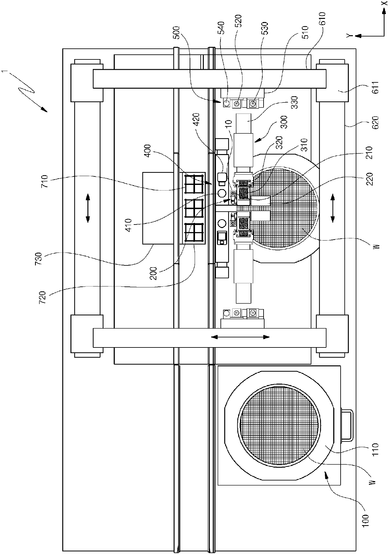
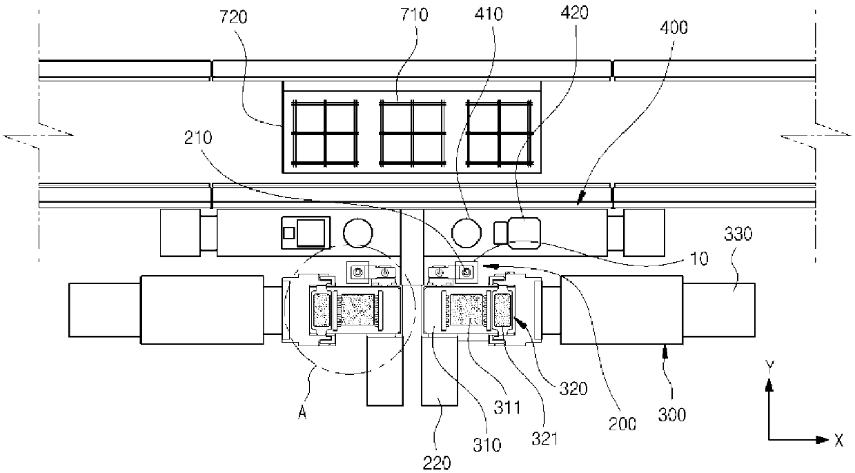
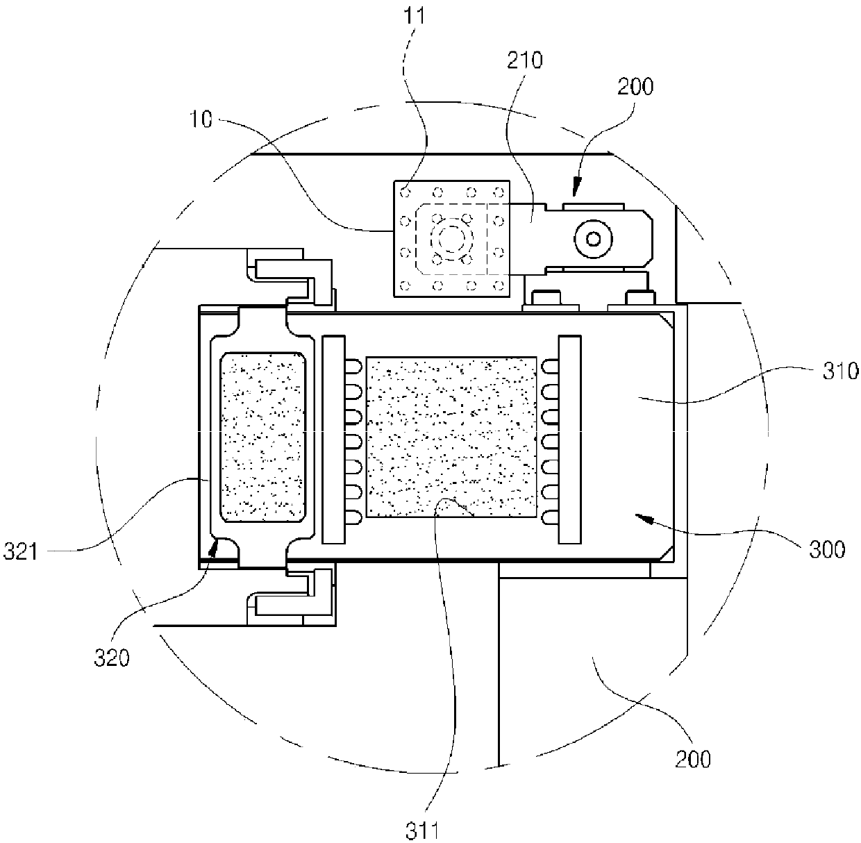
[0068] Hereinafter, embodiments of the present invention will be described in detail with reference to the drawings. The embodiments described below are provided as examples capable of conveying the idea of ​​the present invention to those skilled in the art. The present invention is not limited to the embodiments described below and may be embodied in other ways. In order to clearly describe the present invention, parts irrelevant to the description may be omitted in the drawings, and the sizes of constituent elements, etc. may be enlarged for easy understanding.

[0069] The flip chip bonding process is to use a sawing machine to cut a wafer into a plurality of semiconductor chips (flip chips 10 ), absorb each semiconductor chip, and mount the flip chips 10 on the substrate 710 to be mounted. Process on the bonding site (mounting area) of each semiconductor chip.

[0070] Generally, the bonding process of a flip chip includes the following processes: a process in which the...


PUM


Abstract

The invention relates to a flip-chip bonding device and a bonding method thereof. A flip-chip bonding device according to an embodiment of the present invention includes: a gripping unit for gripping a semiconductor chip from a wafer; a bonding head including a bonding gripper and a substrate viewer; an immersion unit containing a The flux of the bumps provided on the bottom surface of the chip; the up-looking viewer inspects the bottom surface of the semiconductor chip impregnated with flux; the flux viewer inspects the state of the flux accommodated in the dipping unit; the drive unit connects the bonding head and The flux viewer is conveyed to an arbitrary position in the x-y plane; and the bonding table provided with the substrate, wherein the substrate viewer inspects the dipping unit to The state of the flux before dipping of the semiconductor chip is inspected, and the solder viewer inspects the dipping unit to inspect the state of the flux after the dipping of the semiconductor chip during inspection of the chip dipped by the flux by the up-looking viewer.

Description

technical field [0001] The present invention relates to a flip-chip bonding device and a flip-chip bonding method, and in more detail, to a flip-chip that inspects the bonding state of the flip-chip before and after dipping the solder. A chip bonding device and a flip chip bonding method. Background technique [0002] Generally, a process for attaching a semiconductor chip to a circuit substrate needs to be performed very precisely, and a plurality of mounting areas for fixing the semiconductor chip are provided on the substrate. On the other hand, the mounting area of ​​the semiconductor chip and the circuit board should be electrically connected accurately, and the semiconductor chip should be mounted on the exact position (pattern) of the mounting area in order to reduce the defective rate. [0003] The semiconductor chip mounting process described above may be called a bonding process. Depending on the particularity of the process requiring precise work, the semiconduc...

Claims


Application Information

Patent Timeline
Patent Type & Authority Patents(China)
IPC IPC(8): H01L21/60H01L21/66
CPCH01L21/50H01L21/52H01L21/67H01L21/67132H01L21/67144H01L21/67155H01L21/681H01L21/82H01L22/12H01L24/75H01L24/81H01L2221/683H01L24/742H01L2224/742H01L2224/81H01L2224/75H01L22/00
Inventor 郑显权
Owner HANMI SEMICON CO LTD
Why Eureka
Try Eureka