Organic electroluminescent device and preparation method thereof

an electroluminescent device and organic technology, applied in thermoelectric devices, manufacturing tools, vacuum evaporation coatings, etc., can solve the problems of holes, deterioration of device characteristics and lifetime, and difficult to find an example of introducing inorganic matter layers into the inside of light-emitting layers

Inactive Publication Date: 2010-11-18
INKTEC CO LTD
View PDF7 Cites 20 Cited by
  • Summary
  • Abstract
  • Description
  • Claims
  • Application Information

AI Technical Summary

Benefits of technology

[0007]An object of the present invention provides a long-lifetime OLED structure by forming an inorganic oxide interlayer configured of at least one layer between light-emitting layers to increase the recombination probability of electrons-holes injected from its cathode and anode in the light-emitting layers so that the operating voltage of the OLED device is lowered and the efficiency thereof is improved, in order to improve the conventional OLED device characteristics.Technical Solution
[0012]The feature of the present invention is the formation the inorganic oxide interlayer between the light-emitting layers in the process described with reference to FIGS. 1 and 2, but is not limited thereto. It is considered that the inorganic oxide of the present invention forms a net structure by reacting on a surface of light-emitting organic matter under proper conditions. If the inorganic oxide forms well arranged net structure on the organic matter, the characteristics are maximized. The inorganic oxide interlayer serves to maintain constant movement speed of electron and hole to make the mobility of electron and hole in a recombination region slow so that the density of electron and hole becomes high and the recombination probability is increased.

Problems solved by technology

In the case of the organic matter, high voltage is applied so that an organic light-emitting layer with weak molecular structure is damaged due to high energy, thereby deteriorating device's characteristic and lifetime.
Generally, in the case of the organic matter used in the light-emitting layer, the characteristics are deteriorated by holes.
However, it is hard to find an example introducing an inorganic matter layer into the inside of the light-emitting layer.
Furthermore, there has been a limitation in obtaining satisfactory efficiency and lifetime in the case of a conventional OLED structure using an organic matter intermediate layer formed.

Method used


Image

  • Organic electroluminescent device and preparation method thereof
  • Organic electroluminescent device and preparation method thereof
  • Organic electroluminescent device and preparation method thereof

Examples


example 1

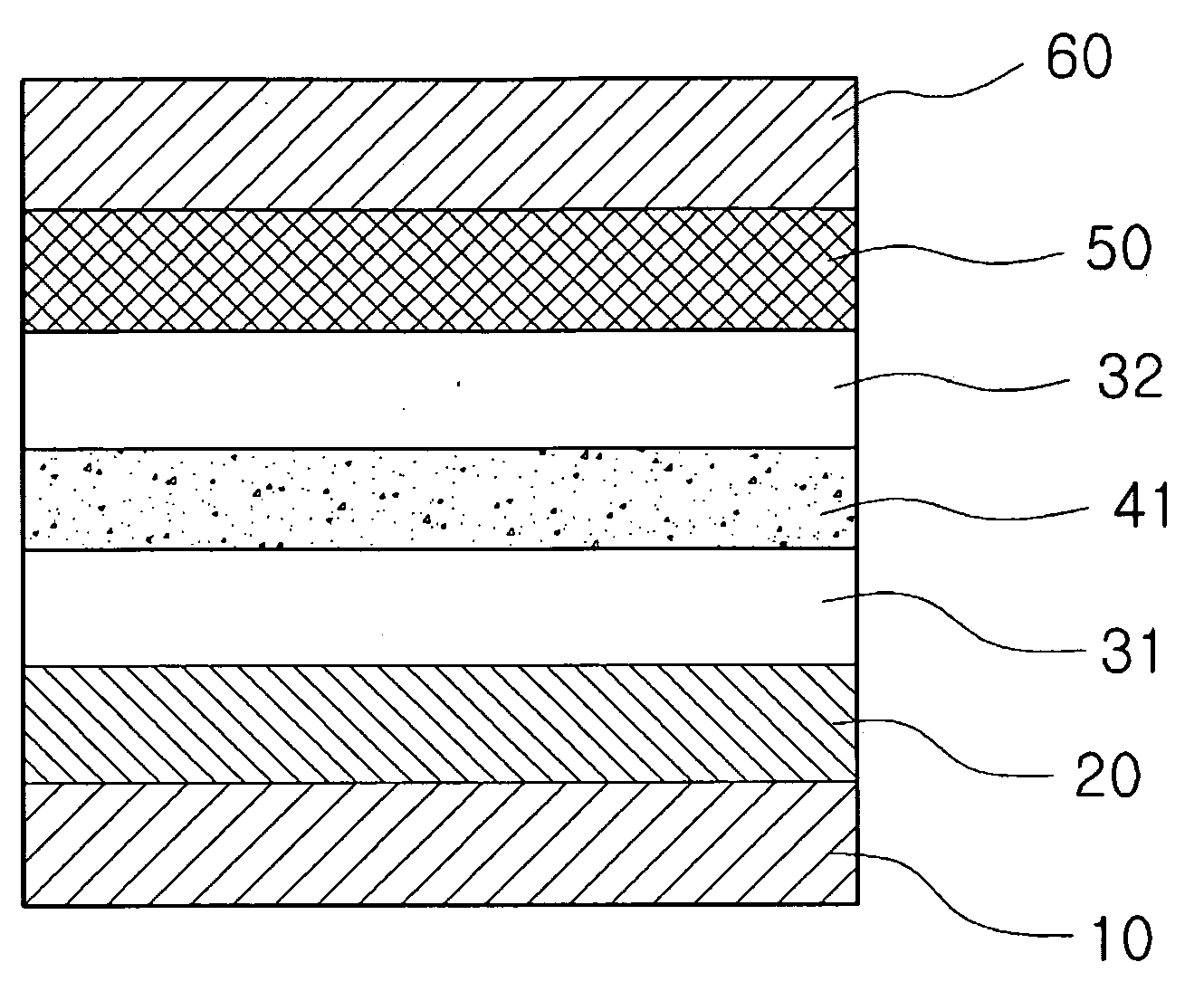
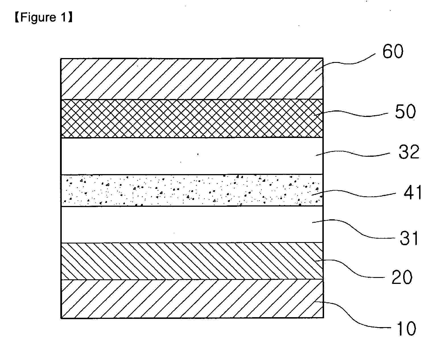
[0035]A 15 Ω / cm2 (120 nm) ITO glass substrate as an anode electrode is cut at a proper size and is cleaned in isopropyl alcohol and pure water by means of ultrasonic wave for 10 minutes and is cleaned by means of UV or ozone for 20 minutes. A PEDOT / PSS (product available from Bayer Co.; Poly(3,4-ethylenedioxythiophene) / Poly(styrene sulfonic acid)) aqueous solution is spin-coated on the upper of the substrate to form a hole injection layer of 40 nm in thickness. Then, a light-emitting layer of 40 nm in thickness is formed on the hole injection layer by spin-coating the mixture of the 95:5 weight percent of PVK (Poly(9-vinylcarbazole) available form Aldrich Co.) and Flrpic (Iridium(III) bis[(4,6-difluorophenyl)pyridinato-N,C2′]picolinate), which is blue phosphor light-emitting material, and a zirconium oxide intermediate layer of 10 nm in thickness is then formed on the upper of the light-emitting layer by spin-coating zirconium oxide solution dissolved with D40 (product form EXXON Co...

example 2

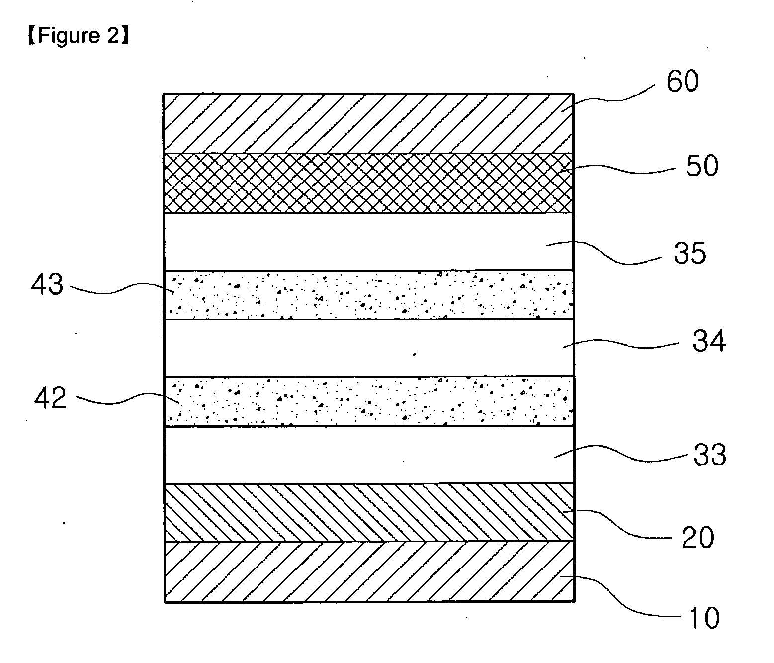
[0036]A 15 Ω / cm2 (120 nm) ITO glass substrate as an anode electrode is cut at a proper size and is cleaned in isopropyl alcohol and pure water by means of ultrasonic wave for 10 minutes and is cleaned by means of UV or ozone for 20 minutes. A PEDOT / PSS (hole injection material which is product from Bayer Co.) aqueous solution is spin-coated on the upper of the substrate to form a hole injection layer of 40 nm in thickness. Then, a light-emitting layer of 40 nm in thickness is formed on the hole injection layer by spin-coating the mixture of the 95:5 weight percent of PVK and Ir(ppy)3 (fac-tris(2-phenylpyridinato)iridium), which is green phosphor light-emitting material, and a zirconium oxide intermediate layer of 10 nm in thickness is then formed on the upper of the light-emitting layer by spin-coating zirconium oxide solution dissolved with D40 (product form EXXON Co.) solvent. Thereafter, the light-emitting layer of 40 nm in thickness is formed on the zirconium oxide intermediate ...

example 3

[0037]A 15 Ω / cm2 (120 nm) ITO glass substrate as an anode electrode is cut at a proper size and is cleaned in isopropyl alcohol and pure water by means of ultrasonic wave for 10 minutes and is cleaned by means of UV or ozone for 20 minutes. A PEDOT / PSS aqueous solution is spin-coated on the upper of the substrate to form a hole injection layer of 40 nm in thickness. Then, a light-emitting layer of 40 nm in thickness is formed on the hole injection layer by spin-coating the mixture of the 95:5 weight percent of PVK and Btp2Ir(acac)(Iridium(III) bis(2-(2′-benzothienyl)pyridinato-N,C3′)(acetylacetonate), which is red phosphor light-emitting material, and a zirconium oxide intermediate layer of 10 nm in thickness is then formed on the upper of the light-emitting layer by spin-coating zirconium oxide solution dissolved with D40 (product form EXXON Co.) solvent. Thereafter, the light-emitting layer of 40 nm in thickness is formed on the zirconium oxide intermediate layer by spin-coating t...


PUM

PropertyMeasurementUnit
thicknessaaaaaaaaaa
thicknessaaaaaaaaaa
thicknessaaaaaaaaaa

Abstract

The present invention relates to a method capable of considerably improving the characteristics of an organic electroluminescent device. The present invention provides a method capable of reducing operating voltage and improving efficiency by inserting an inorganic oxide interlayer configured of at least one layer between light-emitting layers.

Description

TECHNICAL FIELD[0001]The present invention relates to an organic electroluminescent device or an organic light emitting diode (OLED), and more specifically to an organic electroluminescent device or an organic light emitting diode capable of lowering operating voltage and improving efficiency by inserting an inorganic oxide interlayer configured of at least one layer between light-emitting layers.BACKGROUND ART[0002]An OLED is a self-emissive device using a phenomenon generating light itself by combining electron and hole in a light-emitting layer if current is applied to a device including a fluorescent light-emitting layer or a phosphor light-emitting layer between its cathode and anode. The OLED is simple in a structure and a manufacturing process as well as can implement high definition image and wide viewing angle. Also, the OLED can completely implement moving picture and high color purity and has features suitable for portable electronic equipment due to low power consumption...

Claims


Application Information

Patent Timeline
Patent Type & Authority Applications(United States)
IPC IPC(8): H01L51/52H01L51/56C23C14/34B28B11/08
CPCH01L51/5036H05B33/22H05B33/14H01L51/5096H10K85/1135H10K85/146H10K85/60H10K85/631H10K85/324H10K85/342H10K50/125H10K50/131H10K50/18H10K50/11H10K2101/10H10K50/19
Inventor CHO, HYUN-NAMYOO, JI-HOONCHUNG, KWANG-CHOON
Owner INKTEC CO LTD
Why Eureka
Try Eureka