Coated LED with improved efficiency

a technology of led chips and coatings, applied in the direction of discharge tubes luminescnet screens, semiconductor devices for light sources, lighting and heating apparatus, etc., can solve the problems of limiting the package efficiency, different colors for different parts, color separation in the beam pattern, etc., to reduce the blue flux density (w) of the led chip and the effect of reducing the color shift of the led chip

Active Publication Date: 2009-01-20
CONSUMER LIGHTING (U S) LLC
View PDF53 Cites 278 Cited by
  • Summary
  • Abstract
  • Description
  • Claims
  • Application Information

AI Technical Summary

Benefits of technology

[0020]Preferably, a phosphor coating is provided which completely surrounds the LED chip and has a coverage area at least approximately 10 times the exposed area of the absorbing parts of the LED. In most cases, such as when the phosphor is coated on a hemisphere or similar geometry structure, such a requirement is met by removing the phosphor coated surface from the chip by at least a distance 2-3 times the length of the longest side of the chip and surrounding the chip such that no radiation can escape without striking the phosphor coated surface. Radiation generated or reflected off such a coating has an increased probability of striking other parts of the coating rather than the chip, submount, etc. Hence, there is less light lost due to radiation being absorbed by these internal structures of the LED.

Problems solved by technology

In addition because the phosphors typically are not perfect absorbers of long wavelength UV or blue radiation some of the initial excited radiation emitted by the LED chip itself is also reflected back onto the aforementioned structural elements.
The light lost due to absorption of radiation by the LED chip, submount, reflector and lead structure limits the package efficiency.
This results in color separation in the beam pattern.
It also leads to different colors for different parts due to different coating patterns and thicknesses as well as undesirable blue or yellow rings in the LED emission pattern.
Another problem that is encountered in conventional LED packages is that the efficiency of the phosphor is decreased when it is positioned in a layer on top of or adjacent the LED chip.
Still another drawback to conventional LED packages is that, due to the fact that the phosphor coating is applied non-uniformly, the total amount of phosphor used is often more than is necessary for the efficient conversion of the light emitted by the chip.
Phosphor compositions are relatively expensive and this additional amount increases the total cost of the LED significantly.
Nevertheless, the LED chip itself, especially in the case of a chip with a SiC substrate, absorbs significant amounts of both its own radiation and that of the phosphor radiation.
This arrangement reduces non-uniformity in the thickness of the coating over the chip as well as promoting LED to LED color uniformity.
However, it may actually decrease the overall efficiency of the LED because the chip and submount are absorbing and more than half the radiation generated by the phosphor coating is reflected directly back onto these components.

Method used


Image

  • Coated LED with improved efficiency
  • Coated LED with improved efficiency
  • Coated LED with improved efficiency

Examples


Embodiment Construction

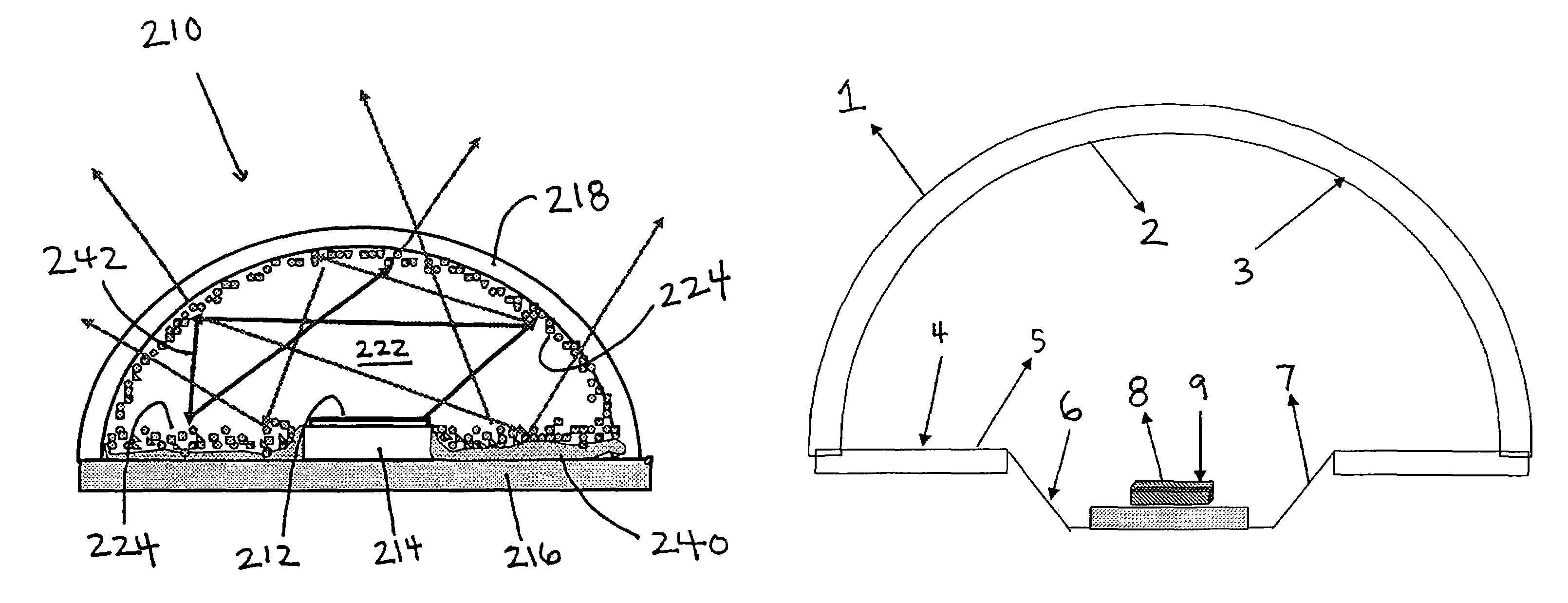
[0032]Although the discussion below with respect to embodiments of the present invention is directed to LEDs for convenience, it should be understood that the invention relates to the use of any light emitting semiconductor. With reference to FIG. 1, a conventional LED assembly is shown generally at 10. The LED assembly includes an LED chip 12 mounted on a bottom surface 14 of the LED assembly. The LED chip 12 emits radiation (typically UV or blue light in a white light LED). A lens 18 made from a transparent material surrounds the chip 12 and bottom surface 14. Two lead wires 20 connect the chip 12 to a source of power. Filling the space 22 between the lens and the chip 12 is typically an epoxy or other transparent material (not shown). Intimately dispersed within the epoxy are phosphor particles (not shown) that absorb at least a portion of the light emitted by the chip 12 and converting it to a different wavelength.

[0033]While the performance of such LEDs can be adequate for some...


PUM


Abstract

An LED device including an LED chip and a lens positioned apart from the chip and coated with a uniform thickness layer of fluorescent phosphor for converting at least some of the radiation emitted by the chip into visible light. Positioning the phosphor layer away from the LED improves the efficiency of the device and produces more consistent color rendition. The surface area of the lens is preferably at least ten times the surface area of the LED chip. For increased efficiency, the reflector and submount can also be coated with phosphor to further reduce internal absorption.

Description

CROSS REFERENCE TO RELATED APPLICATION[0001]This application is a 371 of PCT / US03 / 27363 filed Aug. 29, 2003, which claims benefit of No. 60 / 407,426 filed Aug. 30, 2002, entitled “Coated LED with Improved Efficiency”, the disclosures of which are hereby incorporated by reference herein.BACKGROUND OF THE INVENTION[0002]This invention relates to a light emitting device comprising a UV or blue light emitting diode or laser diode (LED) and an excitable phosphor. More specifically, the present invention relates to a phosphor coated LED having a specific geometry disclosed for the coating designed to improve the efficiency of the LED.[0003]There is currently a market for LED's for general illumination, so called “white LED's”. These “white LED's” emit radiation that appears substantially white to those that perceive it. The most popular white LED's consist of blue emitting GaInN epitaxially grown layers on sapphire (single crystal alumina) or single crystal SiC. The blue emitting chips are...

Claims


Application Information

Patent Timeline
Patent Type & Authority Patents(United States)
IPC IPC(8): H01L29/22H01J63/04H01L29/24H01L33/00H01L21/00H01L33/44H01L33/50H01L33/58
CPCH01L33/507H01L33/58H01L33/44F21K9/56H01L2224/48091F21K9/64H01L2924/00014
Inventor SOULES, THOMAS F.WEAVER, JR., STANTONCHEN, CHEN-LUN HSINGSOMMERS, MATHEWKOLODIN, BORISSETLUR, ANAN ACHYUTSTECHER, THOMAS ELLIOT
Owner CONSUMER LIGHTING (U S) LLC
Why Eureka
Try Eureka