Groove forming method

A trench and stage technology, which is applied in the direction of electrical components, semiconductor/solid-state device manufacturing, circuits, etc., can solve the problems affecting the isolation characteristics of isolation structures, and achieve the effect of enhanced oxidation and weakened etching

Active Publication Date: 2014-10-29
SEMICON MFG INT (SHANGHAI) CORP
View PDF4 Cites 11 Cited by
  • Summary
  • Abstract
  • Description
  • Claims
  • Application Information

AI Technical Summary

Problems solved by technology

[0007] However, when the first trench 104 and the second trench 105 are formed by the above method, the depth of the first trench 104 formed in the first region 11 will be smaller than that of the second region 12 due to the etch loading effect. The depth of the formed second trench 105 affects the isolation characteristics of the formed isolation structure

Method used


Image

  • Groove forming method
  • Groove forming method
  • Groove forming method

Examples


Embodiment Construction

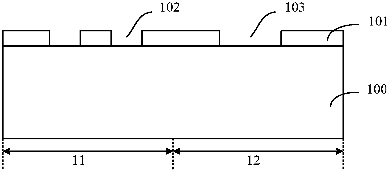
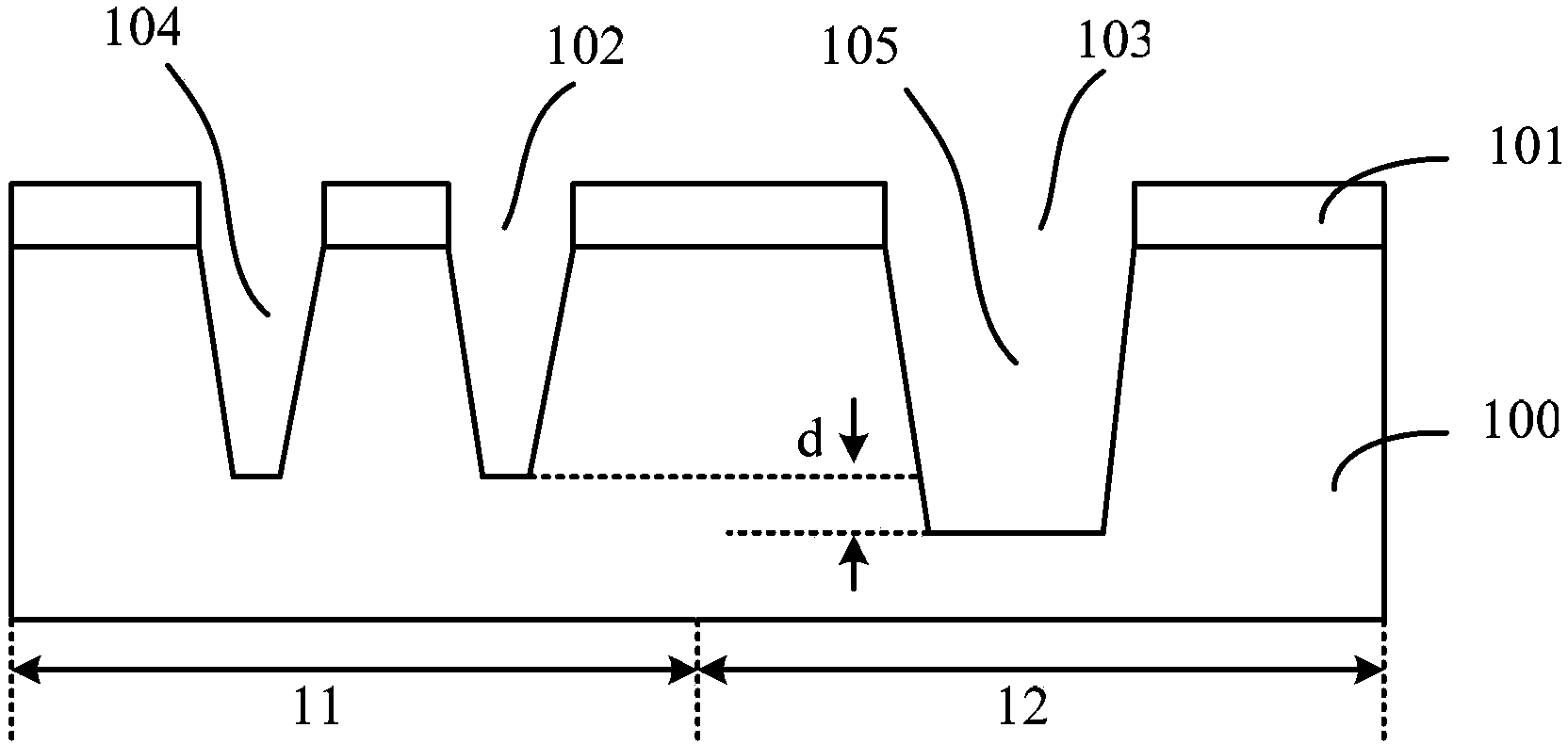
[0033] Please refer to figure 2 , the depth of the first trench 104 formed in the pattern dense area (first region 11 ) is smaller than the depth of the second trench 105 formed in the pattern empty area (second region 12 ) for shallow trenches formed in the prior art.

[0034] The inventors studied the process of forming shallow trenches in the prior art and found that since the width of the first trench 104 formed in the first region 11 is smaller than the width of the second trench 105 formed in the second region 12, the When the semiconductor substrate 100 is etched by a plasma etching process, the exchange rate of the etching plasma and the etching by-products in the first trench 104 will be smaller than that of the etching plasma and the etching by-products in the second trench 105. Exchange rate, thus the etch rate of the semiconductor substrate of the first region 11 will be less than the etch rate of the semiconductor substrate of the second region 12, and in the etc...


PUM


Abstract

A groove forming method comprises the steps of providing a silicon substrate which comprises a first area and a second area; performing plasma etching on the silicon substrate, wherein the plasma etching comprises the steps of performing etching of a first stage, forming a first opening and a second opening in the silicon substrate, and enabling the width of the first opening to be smaller than that of the second opening; performing oxidation of a second stage, forming a first oxidation layer at the bottom and a side wall of the first opening, forming a second oxidation layer at the bottom and a side wall of the second opening; performing etching of a third stage, etching and removing the first oxidation layer and the second oxidation layer of a partial thickness; performing etching of a fourth stage, forming a third opening and a fourth opening; and repeating the steps of oxidation of the second stage, etching of the third stage and etching of the fourth stage until a plurality of first grooves are formed in the first area of the silicon substrate and a plurality of second grooves are formed in the second area of the substrate. The influence on the etching process caused by the etching load effect is effectively eliminated.

Description

technical field [0001] The invention relates to the field of semiconductor manufacturing, in particular to a method for forming a trench. Background technique [0002] With the progress of semiconductor technology, shallow trench isolation (Shallow Trench Isolation, STI) method has gradually replaced other isolation structures such as local silicon oxidation method used in traditional semiconductor device manufacturing. Compared with other isolation directions, the shallow trench isolation method has many advantages, mainly including: 1. The shallow trench isolation method can obtain a narrower isolation width of semiconductor devices, thereby increasing the device density; 2. Shallow trench isolation The method can improve the flatness of the surface, so that the minimum line width can be effectively controlled during photolithography. [0003] For existing methods of forming trench isolation structures, please refer to Figure 1 ~ Figure 2 . [0004] First, please refer ...

Claims


Application Information

Patent Timeline
Patent Type & Authority Applications(China)
IPC IPC(8): H01L21/762
CPCH01L21/76205
Inventor 王新鹏
Owner SEMICON MFG INT (SHANGHAI) CORP
Why Eureka
Try Eureka