Semiconductor etching method and semiconductor etching system

An etching system and semiconductor technology, applied in semiconductor/solid-state device manufacturing, semiconductor/solid-state device testing/measurement, electrical components, etc., can solve problems such as ineffective reduction of errors, device differences, and inability to reduce errors. Achieve the effect of improving etching precision, reducing error and reducing depth difference

Active Publication Date: 2012-05-23
SEMICONDUCTOR MANUFACTURING INTERNATIONAL (BEIJING) CORP
View PDF3 Cites 0 Cited by
  • Summary
  • Abstract
  • Description
  • Claims
  • Application Information

AI Technical Summary

Problems solved by technology

With the reduction of feature size in semiconductor manufacturing, the allowable error range is getting smaller and smaller, so this method of setting the error range to detect the etching result cannot accurately control the accuracy of etching
Because this method only performs feedback when the line width does not meet the requirements to adjust the etching parameters, and does not adjust the parameters if the requirements are met, so this method can only maintain the error within a certain range and cannot effectively reduce the error.
Moreover, with this method, even if the groove line width meets the requirements, there may be a large difference between the grooves etched at the same time, so that there is a large difference between the manufactured devices.
[0004] Similarly, there are errors that cannot be reduced in the etching of other etching patterns, and there may be large differences between the etching patterns that are not etched at the same time, so that there are large differences between the manufactured devices The problem

Method used


Image

  • Semiconductor etching method and semiconductor etching system
  • Semiconductor etching method and semiconductor etching system
  • Semiconductor etching method and semiconductor etching system

Examples


Embodiment Construction

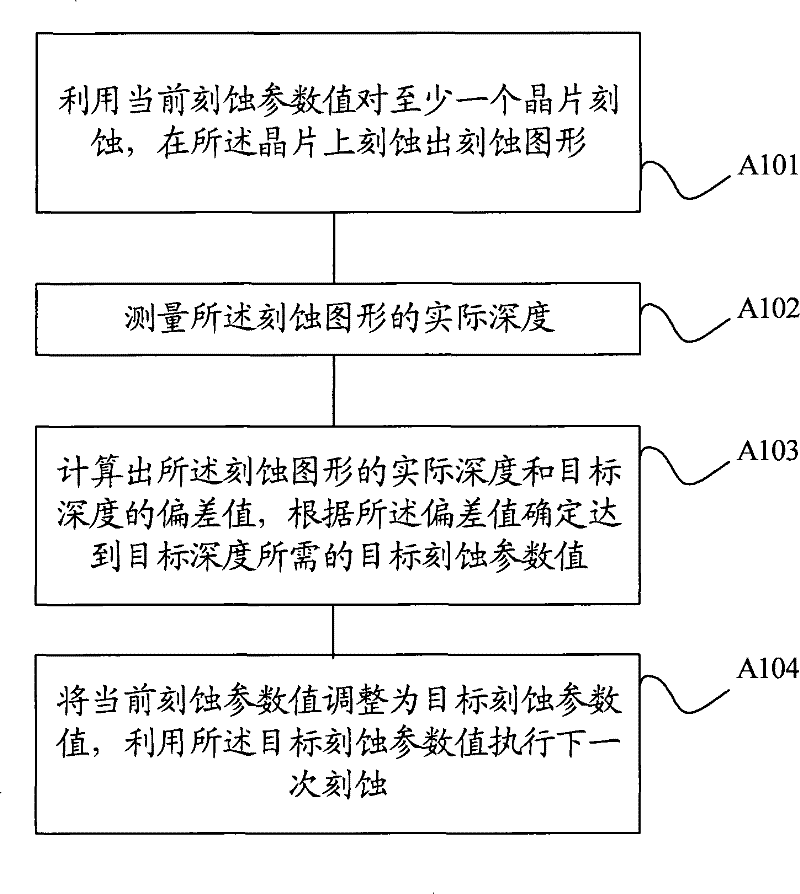
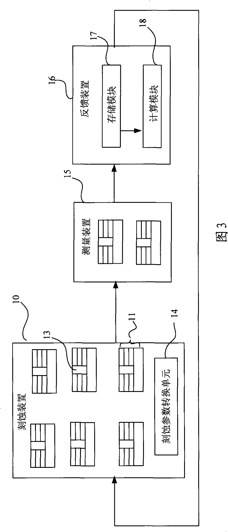
[0033] In order to make the above-mentioned purposes, features and advantages of the present invention more obvious and understandable, the specific implementation modes of the present invention will be described in detail below in conjunction with the accompanying drawings, so that the above-mentioned and other purposes, features and advantages of the present invention will be clearer. Like reference numerals designate like parts throughout the drawings. The drawings have not been drawn to scale, emphasis instead being placed upon illustrating the gist of the invention.

[0034] For clarity, in the following description, well-known functions and constructions are not described in detail since they would obscure the invention with unnecessary detail. It should be appreciated that in the development of any actual embodiment, numerous implementation details must be worked out to achieve the developer's specific goals, such as changing from one embodiment to another in accordance...


PUM


Abstract

The invention provides a semiconductor etching method and a semiconductor etching system. The method comprises the following steps: etching at least one wafer by utilizing current etching parameter values, etching etched patterns on the wafer; measuring the real depth of the etched patterns; calculating the deviation value of the real depth and the target depth, determining target etching parameter values needed by reaching the target depth according to the deviation value; adjusting the current etching parameter values to be the target etching parameter values, and executing the next etchingby using the target etching parameter values. The semiconductor etching system comprises an etching device, a measuring device and a feedback device. The semiconductor etching method and the semiconductor etching system can reduce the error during the etching, improve the etching accuracy of the etched patterns and reduce the difference among the etched patterns during different etchings.

Description

technical field [0001] The invention relates to the technical field of semiconductor manufacturing, in particular to a semiconductor etching method and an etching system. Background technique [0002] As the feature size of the device shrinks, the precision requirement for the device manufacturing is getting higher and higher. During semiconductor manufacturing, unwanted material is removed from the wafer surface by etching. Etching requirements depend on the type of feature pattern to be produced, such as aluminum alloy wiring, polysilicon gate, shallow trench isolation region. Due to the complex structure of the device, the wafer has a large number of materials requiring different etching parameters, which makes it difficult to control the accuracy of etching. At the same time, etching is affected by many external conditions such as air pressure, power supply, etching gas content, gas flow distribution of etching gas in the etching chamber, and etching time, so it is dif...

Claims


Application Information

Patent Timeline
Patent Type & Authority Patents(China)
IPC IPC(8): H01L21/3065H01L21/66
Inventor 赵林林
Owner SEMICONDUCTOR MANUFACTURING INTERNATIONAL (BEIJING) CORP
Why Eureka
Try Eureka