Slot array PCB (printed circuit board) antenna

A PCB antenna, slot array technology, applied in slot antennas, antennas, antenna arrays and other directions, can solve the problems of low gain, low directivity, and difficult integration of PCB antennas, and achieve small size, good directivity, and high gain. Effect

Active Publication Date: 2014-10-29
SUZHOU HUASHI WIRELESS TECH
View PDF5 Cites 6 Cited by
  • Summary
  • Abstract
  • Description
  • Claims
  • Application Information

AI Technical Summary

Problems solved by technology

However, the current PCB antennas usually have low gain, low directivity, large size, heavy weight and difficult integration

Method used


Image

  • Slot array PCB (printed circuit board) antenna
  • Slot array PCB (printed circuit board) antenna
  • Slot array PCB (printed circuit board) antenna

Examples


Embodiment

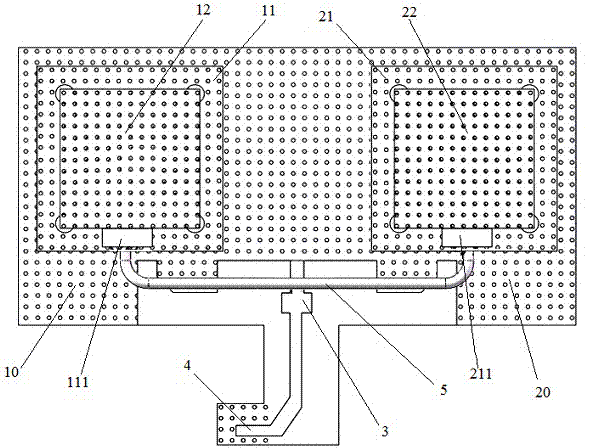
[0026] like figure 1 As shown, the slot array PCB antenna disclosed in the present invention includes an integrated first reflector 10 and a second reflector 20, and the first radiating unit layer 11 and the first Director 12, the second radiating element layer 21 and the second director 22 are sequentially provided above the second reflector 20; the connection between the first reflector 10 and the second reflector 20 passes through a transmission line transformer 3 Connect the stub frequency selection network 4, the first radiating unit layer 11 and the second radiating unit layer 21 are respectively provided with a first feeder access point 111 and a second feeder access point 211, the two feeder access points The entry point is connected by a coaxial transmission line 5; the first reflector 10, the second reflector 20, the first radiating element layer 11, the second radiating element layer 21, the first director 12 and the second director 22 Both are PCB structures, a...


PUM


Abstract

The invention discloses a slot array PCB antenna. The slot array PCB antenna comprises a first reflector and a second reflector which are designed integrally; a first radiating element layer and a first director are sequentially arranged above the first reflector, and a second radiating element layer and a second director are sequentially arranged above the second reflector; the connection portion between the first reflector and the second reflector is connected with a stub frequency selective network through a transmission line transformer, and the first radiating element layer and the second radiating element layer are respectively provided with a first feeder access point and a second feeder access point which are connected through a coaxial transmission line, the reflectors, the radiating element layers and the directors are all of a double-sided copper clad PCB structure, and a metalized through hole array is distributed in the double-sided copper clad board. The slot array PCB antenna has the advantages of good directivity and high gain of a yagi antenna as well as small size, light weight, low cost, high performance, integration and installation easiness and the like of a common planar antenna.

Description

technical field [0001] The invention relates to a radio technology, in particular to a slot array PCB antenna. Background technique [0002] In radio technology equipment that transmits information by electromagnetic waves, such as radio, television, communications, navigation, radar, etc., PCB antennas are an essential and important part. In high-efficiency satellites, aircraft and mobile communication mobile phone applications, PCB antennas are higher favor. However, current PCB antennas usually have low gain, low directivity, large size, heavy weight, and difficulty in integration. Contents of the invention [0003] The object of the present invention is to provide a PCB antenna with higher gain, good directivity, small size, light weight and easy integration. [0004] Technical scheme of the present invention is: [0005] The advantages of the present invention are: [0006] A slot array PCB antenna, comprising an integrated first reflector and a second ...

Claims


Application Information

Patent Timeline
Patent Type & Authority Applications(China)
IPC IPC(8): H01Q1/36H01Q1/38H01Q13/10H01Q21/00
Inventor 高怀李昕朱向伟周智俐
Owner SUZHOU HUASHI WIRELESS TECH
Why Eureka
Try Eureka