A booster circuit and its signal output method

A boost circuit and signal technology, applied in the direction of output power conversion device, DC power input conversion to DC power output, electrical components, etc., can solve the problem that the frequency shaking effect cannot be fully exerted, the EMI performance of the power system will deteriorate, Frequency shaking effect is not obvious, etc., to alleviate the effect of EMI problems

Active Publication Date: 2017-05-10
VERTIV CORP
View PDF3 Cites 0 Cited by
  • Summary
  • Abstract
  • Description
  • Claims
  • Application Information

AI Technical Summary

Problems solved by technology

[0004] However, when the input voltage of the above configuration structure is an AC voltage, since the amplitude of the output ripple component is proportional to the size of the load, when the load of the Boost circuit is light, the amplitude of the output ripple component is also small. The frequency shaking effect of the stage is not obvious, and the EMI performance of the power system may still not be ideal; if the input voltage of the above structure configuration becomes a DC voltage, the ripple component of the voltage signal output by the Boost circuit that is twice the frequency of the input AC voltage disappears. The frequency shaking effect of the subsequent LLC topology circuit cannot be fully utilized, and the EMI performance of the power system will deteriorate even more.

Method used


Image

  • A booster circuit and its signal output method
  • A booster circuit and its signal output method
  • A booster circuit and its signal output method

Examples


Embodiment 1

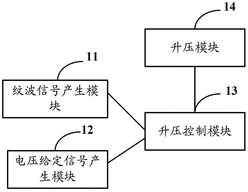
[0038] like figure 1 As shown, it is a schematic structural diagram of the boost circuit in Embodiment 1 of the present invention. The boost circuit includes: a ripple signal generation module 11, a voltage given signal generation module 12, a boost control module 13, and a boost module 14 ;

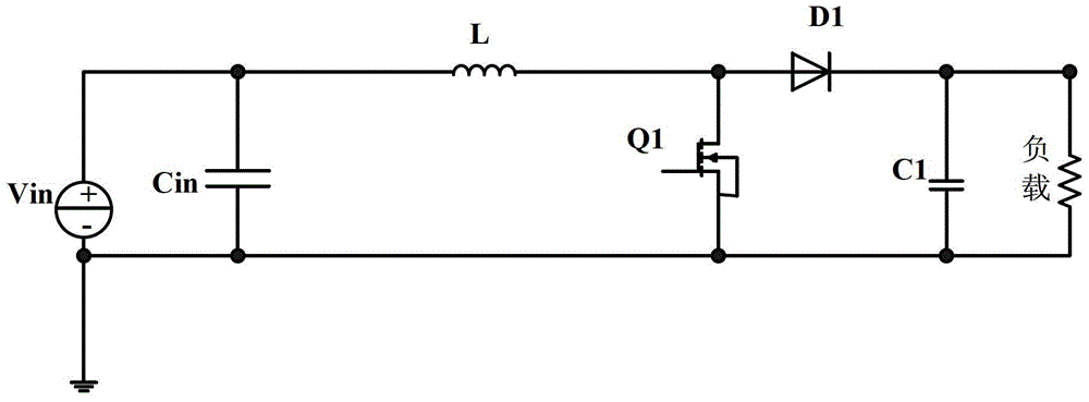
[0039] Wherein, the boost module 14 includes an inductor and a diode serially connected in series between the positive pole of the power supply and the positive pole of the circuit output terminal, and also includes a switch tube and an output filter capacitor, the drain of the switch tube is connected to the anode of the inductor and the diode Between, the source is connected between the negative pole of the power supply and the negative pole of the circuit output terminal, and the output filter capacitor is connected between the cathode of the diode and the source of the switch tube;

[0040] The ripple signal generating module 11 is connected to the boost control module for generatin...

Embodiment 2

[0108] On the basis of the boost circuit provided in Embodiment 1 of the present invention, the embodiment of the present invention provides a signal output method for the boost circuit in Embodiment 1, the flow chart of which is as follows Figure 17 shown, including the following steps:

[0109] Step 101: generating and outputting a given voltage signal and a ripple signal respectively;

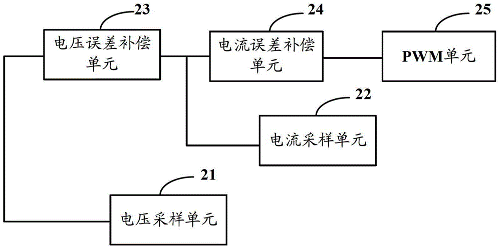
[0110] Step 102: Sampling the inductor current and the output voltage signal, and generating a driving pulse signal according to the ripple signal, the given voltage signal, the sampled voltage signal and the inductor current signal;

[0111] Step 103: Under the control of the driving pulse signal, complete the step-up change of the input voltage signal and provide a DC voltage signal output with a ripple component.

[0112] The specific implementation of the above step 102 can be but not limited to the following three methods:

[0113] like Figure 18 As shown, it is a flow chart of the...


PUM


Abstract

The invention discloses a boosted circuit and a signal output method. The boosted circuit comprises a boosted module, a boosted control module, a ripple signal generation module and a voltage given signal generation module. The boosted control module carries out sampling on an inductance current signal of the boosted module and an output voltage signal. According to a ripple signal, a voltage given signal, the voltage signal and the inductance current signal, wherein the voltage signal and the inductance current signal are acquired through sampling, a driving pulse signal is generated. The boosted module completes a boost change to an input voltage signal under the control of the driving pulse signal and provides direct voltage signal output possessing a ripple component. Because the ripple signal generation module is newly added, the boosted module outputs a voltage signal possessing the ripple component. A backward-stage direct current / direct current link directly generates a jitter frequency effect because the input voltage signal possessing the ripple component so that an electromagnetic interference problem of a power supply system is alleviated.

Description

technical field [0001] The invention relates to the technical field of switching power supplies, in particular to a boost circuit and a signal output method thereof. Background technique [0002] The frequency shaking technology can effectively make the electromagnetic interference (Electromagnetic Interference, EMI) disturbance signal of the equipment evenly divided in a wider frequency spectrum, so that the equipment can easily pass the relevant electromagnetic compatibility (Electromagnetic Compatibility, EMC) test standard, which is conducive to solving the entire The EMI problem of switching power supply system is favored by switching power supply engineers. [0003] The mainstream configuration of the current communication rectifier module power supply system is a power factor correction (Power Factor Correction, PFC) link + DC / DC (DC / DC) link. The PFC link is the (AC / DC) AC / DC link, which converts the AC input voltage into a DC high voltage with a set amplitude (such...

Claims


Application Information

Patent Timeline
Patent Type & Authority Patents(China)
IPC IPC(8): H02M3/155H02M1/44
Inventor 刘兆元
Owner VERTIV CORP
Why Eureka
Try Eureka