Image sensor pixel with changeable conversion gain and working method thereof

An image sensor and conversion gain technology, applied in image communication, color TV parts, TV system parts, etc., can solve the problems of reducing the output image quality of the sensor, difficult to collect, etc., to improve image quality and delay saturation the effect of time

Inactive Publication Date: 2014-11-05
BEIJING SUPERPIX MICRO TECHNOLOGY CO LTD
View PDF5 Cites 2 Cited by
  • Summary
  • Abstract
  • Description
  • Claims
  • Application Information

AI Technical Summary

Problems solved by technology

In the outdoor environment, the linear sensor is not easy to collect the physical informat

Method used


Image

  • Image sensor pixel with changeable conversion gain and working method thereof
  • Image sensor pixel with changeable conversion gain and working method thereof
  • Image sensor pixel with changeable conversion gain and working method thereof

Examples


specific Embodiment

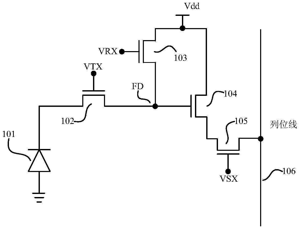
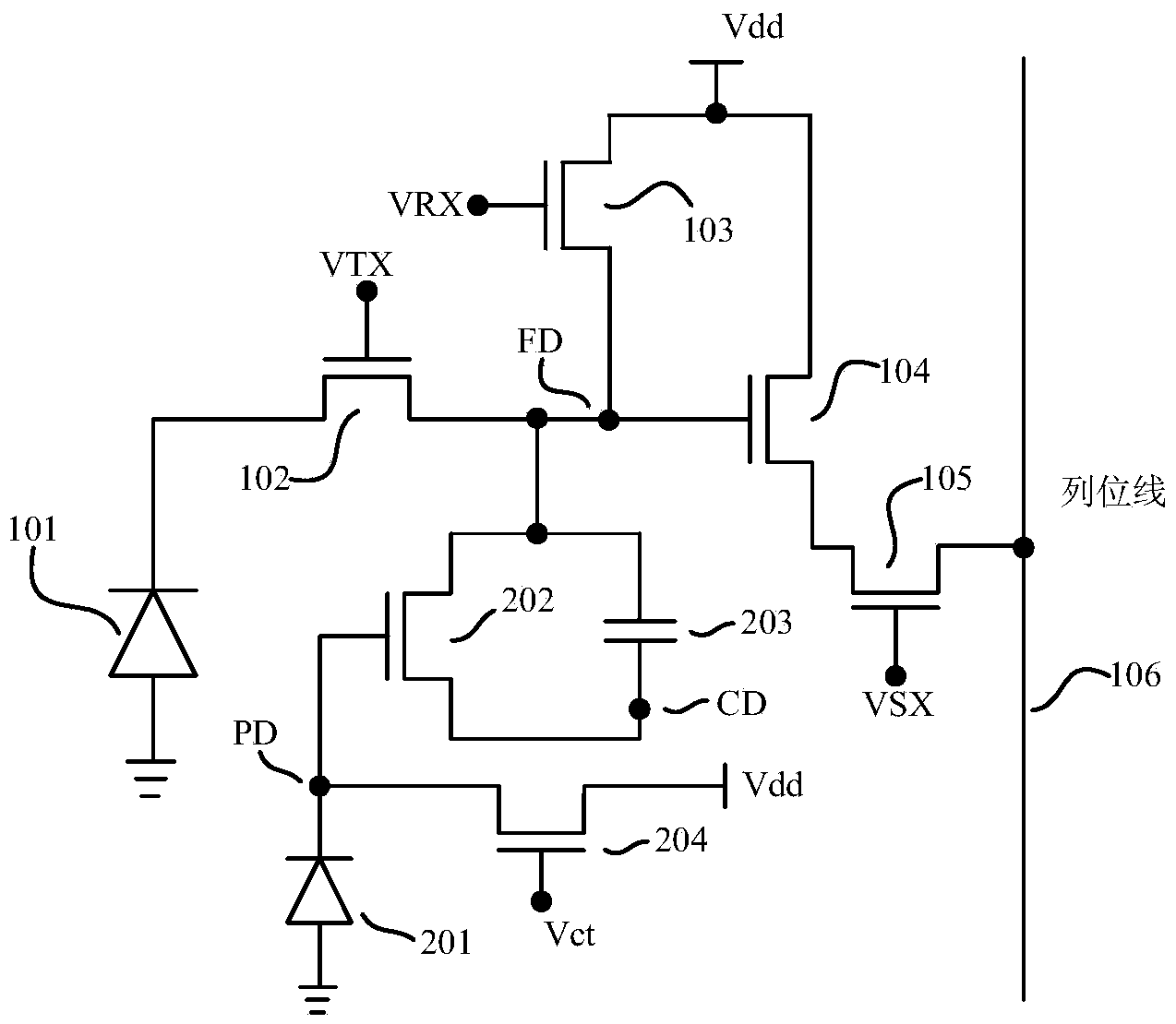
[0046] A special device structure is introduced to the floating active region on the basis of the image sensor pixel of the prior art, such as figure 2 As shown, 101-106 are image sensor pixel devices in the prior art, and VTX, VRX, and VSX are gate terminals of 102, 103, and 105 respectively; 201 is a second photodiode, 202 is a switching transistor, 203 is a capacitor, and 204 is a For the second reset transistor, PD is the gate terminal of 202 , CD is one terminal of 203 , Vdd is the power supply, and Vct is the gate terminal of 204 . Such as figure 2 As shown, the charge collection end of 201 is connected to PD, the source end of 204 is connected to PD, and the drain end of 204 is connected to Vdd; the drain end of 202 is connected to FD, and the source end of 202 is connected to CD; the other end of 203 is connected to FD is connected. Among them, 101 and 201 are N-type photodiodes, 102-105, 202, and 204 are N-type transistors; 202 and 204 are low-threshold transistor...


PUM

PropertyMeasurementUnit
Capacitanceaaaaaaaaaa

Abstract

The invention discloses an image sensor pixel with the changeable conversion gain and a working method thereof. The image sensor pixel comprises a first photodiode, a charge transmission transistor, a first reset transistor, a source following transistor, a selection transistor, a floating active area, a second photodiode, a second reset transistor, a capacitor and a switch transistor which are arranged in a semiconductor substrate. The drain electrode end of the switch transistor is connected with the floating active area, the source electrode end of the switch transistor is connected with one electrode end of the capacitor, the grid electrode end of the switch transistor is connected with the second photodiode, the other electrode end of the capacitor is connected with the floating active area, the source electrode end of the second reset transistor is connected with the second photodiode, and the drain electrode end of the second reset transistor is connected with a power source. The photovoltaic conversion gain for lowering the sensor pixel in the high illumination environment is used for achieving the purpose of delaying the pixel saturation time, the problem that in the prior art, real object information in the outdoor high illumination environment cannot be easily collected is solved, and the quality of images output by an image sensor is improved.

Description

technical field [0001] The invention relates to an image sensor pixel, in particular to an image sensor pixel with variable conversion gain and a working method thereof. Background technique [0002] Image sensors have been widely used in digital cameras, mobile phones, medical devices, automobiles and other applications. In particular, the rapid development of the technology for manufacturing CMOS (Complementary Metal Oxide Semiconductor) image sensors has made people have higher requirements for the output image quality of the image sensor. [0003] In the prior art, a CMOS image sensor generally adopts a pixel structure with a linear photoelectric response function. Such as figure 1 Shown are CMOS image sensor pixels, also known in the art as 4T (four transistor) active pixels. The components of a 4T active pixel include: a photodiode 101, a charge transfer transistor 102, a reset transistor 103, a source follower transistor 104, a row selection transistor 105, and a c...

Claims


Application Information

Patent Timeline
IPC IPC(8): H04N5/374H04N5/378
Inventor 郭同辉旷章曲
Owner BEIJING SUPERPIX MICRO TECHNOLOGY CO LTD
Why Eureka
Try Eureka