Die bonder and method for detecting positions of bonding tool and semiconductor die relative to each other

A bonding tool and relative position technology, applied in semiconductor devices, semiconductor/solid-state device manufacturing, instruments, etc., can solve problems such as complex optical system composition, and achieve the effect of simple composition

Active Publication Date: 2014-11-05
SHINKAWA CO LTD
View PDF6 Cites 0 Cited by
  • Summary
  • Abstract
  • Description
  • Claims
  • Application Information

AI Technical Summary

Problems solved by technology

Therefore, it is necessary to use a large number of half mirrors or prisms in the optical system, and there is a problem that the composition of the optical system becomes complicated.

Method used


Image

  • Die bonder and method for detecting positions of bonding tool and semiconductor die relative to each other
  • Die bonder and method for detecting positions of bonding tool and semiconductor die relative to each other
  • Die bonder and method for detecting positions of bonding tool and semiconductor die relative to each other

Examples


Embodiment Construction

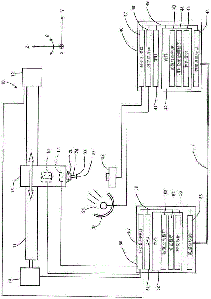
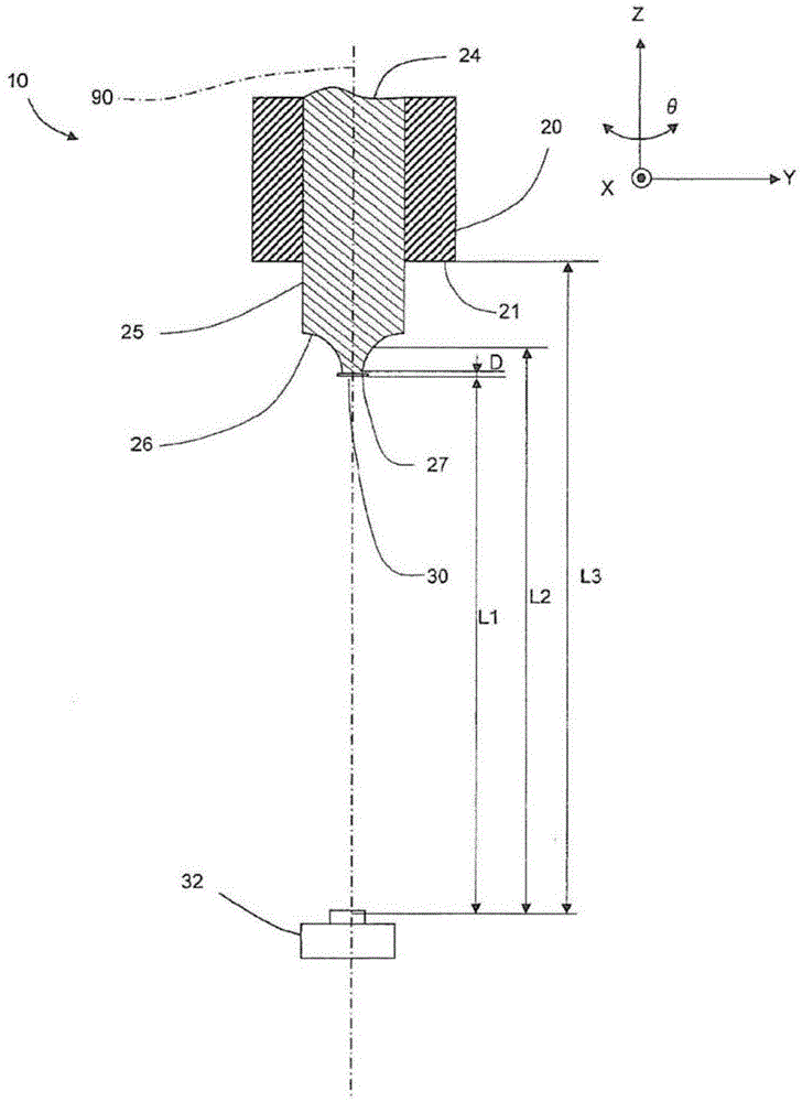
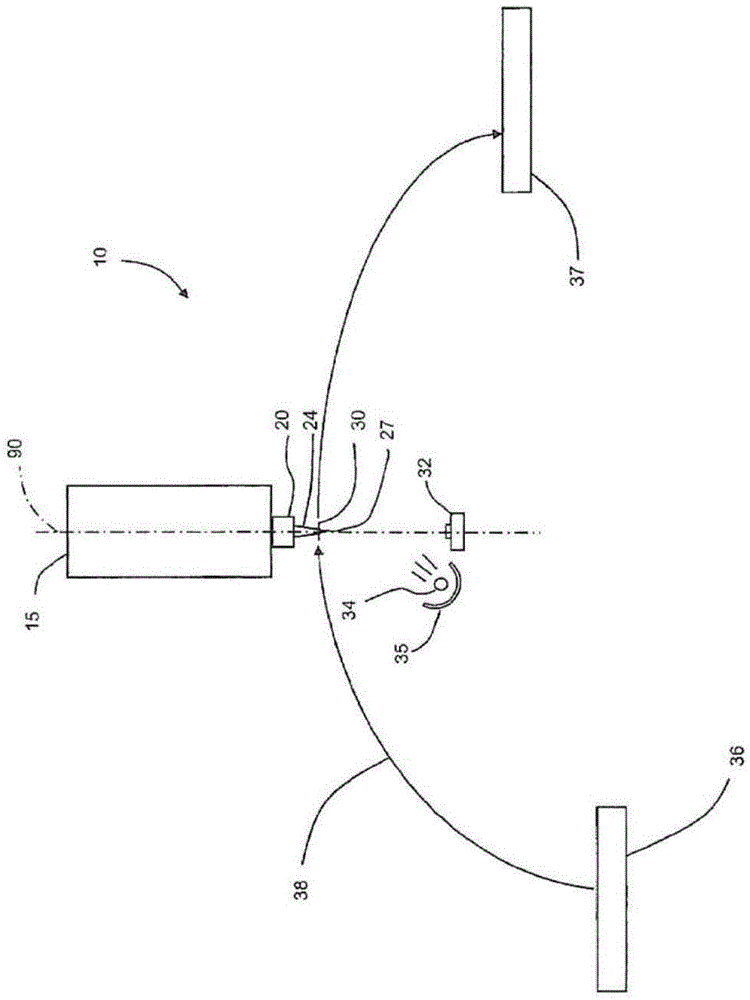
[0033] Hereinafter, embodiments of the present invention will be described with reference to the drawings. like figure 1 As shown, the die bonder 10 of the present invention has a bonding head 15 on which a bonding tool 24 is installed through a crank 20, a guide rail 11 for guiding the bonding head 15 in the Y direction, and a Y direction for moving the bonding head 15 in the Y direction. Moving mechanism 13, X-direction moving mechanism 12 for moving guide rail 11 and bonding head 15 in X direction, camera 32 provided under bonding head 15, flashlight 34 as light source, image processing unit connecting camera 32 and flashlight 34 40, and the control unit 50 connected to the X and Y direction moving mechanisms 12 and 13. The bonding tool 24 has an adsorption surface 27 for adsorbing the semiconductor die 30 at its tip, and the strobe lamp 34 includes a reflector 35 for directing emitted light toward the bonding tool 24 . The bonding head 15 internally includes a Z-directio...


PUM


Abstract

A die bonder contains a bonding tool (24), a strobe (34), a camera (32), and a shank (20). The bonding tool (24) has the following: a tip suction surface (27) that holds a semiconductor die (30) by suction; a base that is wider than said tip suction surface (27); and a sloped surface that connects the suction surface (27) to the base and is sloped with respect to a lengthwise centerline. The camera (32) simultaneously acquires an image of the semiconductor die (30) held by the suction surface (27), an image of the shank (20), and an image of the sloped surface of the bonding tool (24). The shank (20) is in contact with the base of the bonding tool (24), is separated from the suction surface (27) by a distance greater than the depth of focus of the camera (32) in the lengthwise direction of the bonding tool (24), does not move relative to the bonding tool (24), and reflects light from the strobe (34). Misalignment between a semiconductor die and a bonding tool in a die bonder can thus be detected effectively with a simple configuration.

Description

technical field [0001] The invention relates to a structure of a die bonder and a method for detecting the relative position of a bonding tool and a semiconductor crystal grain adsorbed at the front end of the bonding tool. Background technique [0002] A die bonder is often used as an apparatus for bonding a semiconductor die to a circuit board such as a lead frame. The die bonder lowers the semiconductor die sucked and held at the tip of the bonding tool toward the surface of the circuit substrate sucked and fixed on the bonding stage, and bonds the semiconductor die to the circuit board. [0003] In the die bonder, it is necessary to press the semiconductor die to the circuit board in a state where the position of the semiconductor die adsorbed by the bonding tool is aligned with the bonding position of the circuit board. Therefore, when the semiconductor die is transferred by the bonding tool, the relative position of the semiconductor die and the circuit board is align...

Claims


Application Information

Patent Timeline
Patent Type & Authority Applications(China)
IPC IPC(8): H01L21/52G01B11/00
CPCH01L24/75H01L2224/75753H01L2224/75745H01L21/6838H01L21/681
Inventor 辻正人梅原冲人比留间圭一浦桥亮
Owner SHINKAWA CO LTD
Why Eureka
Try Eureka