Optimum operating voltage test method of avalanche photodiode
An avalanche photoelectric, working voltage technology, applied in the direction of single semiconductor device testing, etc., can solve the problem of not being able to respond to other tasks in real time
- Summary
- Abstract
- Description
- Claims
- Application Information
AI Technical Summary
Problems solved by technology
Method used
Image
Examples
Embodiment Construction
[0013] In order to make the objects, features and advantages of the present invention more comprehensible, specific implementations of the present invention will be described in detail below in conjunction with the accompanying drawings.
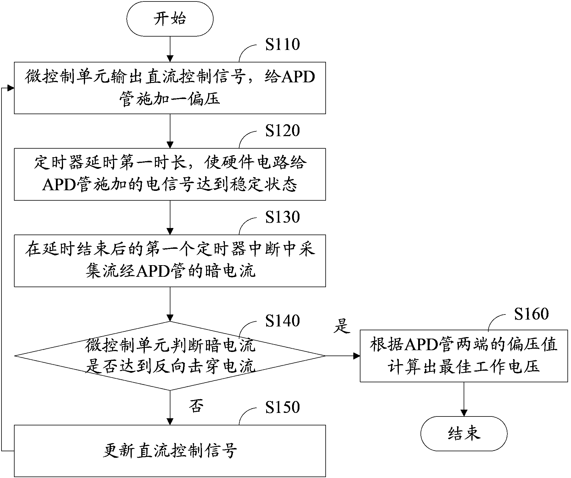
[0014] The method for testing the optimum working voltage of the avalanche photodiode of the present invention adopts the mode of time slice rotation, and can quickly and accurately find the optimum working voltage of the APD tube.
[0015] figure 1 It is a flowchart of a test method for the optimum working voltage of an avalanche photodiode in an embodiment, comprising the following steps:
[0016] S110, the micro control unit outputs a DC control signal, and applies a bias voltage corresponding to the value of the DC control signal to the APD tube.
[0017] The micro control unit outputs an initial DC control signal (DAC signal), and controls the corresponding hardware circuit to apply a bias voltage to the APD tube.
[0018] S120, the t...
PUM
 Abstract
Description
Claims
Application Information
