Charge storage structure, manufacturing method thereof and nonvolatile memory structure
A technology of charge storage and manufacturing method, applied in the direction of electric solid devices, circuits, electrical components, etc., can solve the problems of shrinking, lateral etching acceleration of etching process, etc., to achieve the best reliability and avoid the effect of reducing key dimensions
- Summary
- Abstract
- Description
- Claims
- Application Information
AI Technical Summary
Problems solved by technology
Method used
Image
Examples
Embodiment Construction
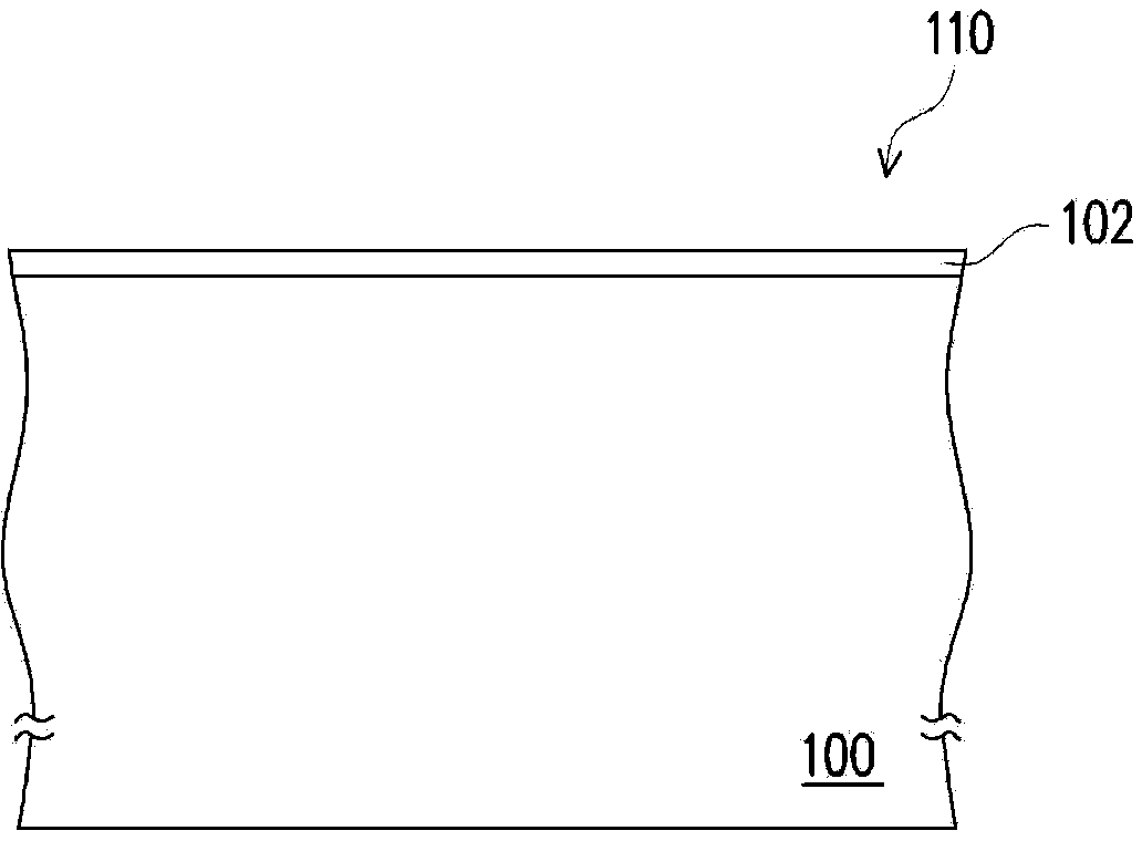
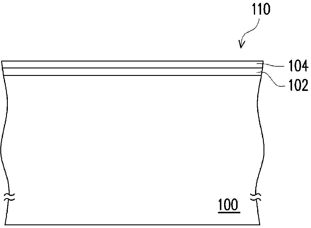
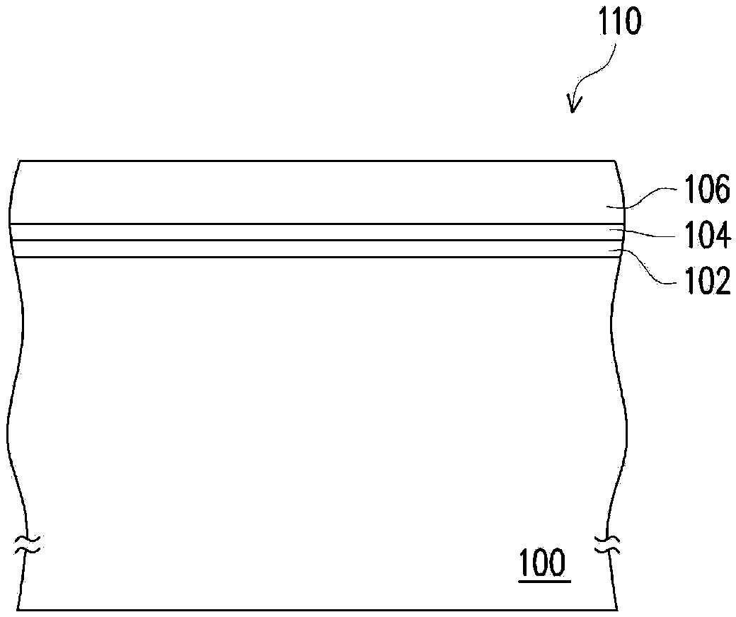
[0033] Figure 1A to Figure 1D Shown is a flow chart of the fabrication of the charge storage structure according to an embodiment of the present application.
[0034] First, please refer to Figure 1A , forming a dielectric layer 102 on the substrate 100, the dielectric layer 102 can be used as a tunneling dielectric layer. The substrate 100 is, for example, a silicon substrate. The material of the dielectric layer 102 is, for example, silicon oxide. The forming method of the dielectric layer 102 is, for example, a thermal oxidation method.
[0035] Next, please refer to Figure 1B , forming a first undoped charge storage layer 104 on the dielectric layer 102 . The first undoped charge storage layer 104 can be used as a shielding layer, which can be used to isolate the dielectric layer 102 from the subsequently formed doped charge storage layer, so as to prevent the doped charge storage layer from covering the dielectric layer. Impurities on the electrical layer form pro...
PUM
 Abstract
Description
Claims
Application Information


