Programming method for flash memory device

A flash memory device and programming method technology, applied in static memory, read-only memory, instruments, etc., can solve the problems of flash memory device upgrade and key size reduction, large depletion layer width, device punch-through, etc., to improve reliability, increase Cell density, the effect of increasing storage capacity and density

Active Publication Date: 2014-12-03
SHANGHAI HUALI MICROELECTRONICS CORP
View PDF5 Cites 1 Cited by
  • Summary
  • Abstract
  • Description
  • Claims
  • Application Information

AI Technical Summary

Problems solved by technology

[0005] However, there is another problem in the technical solution in the above-mentioned patent: because the voltage applied to the drain terminal is relatively high, the width of the depletion layer extending from the drain terminal to the substrate is relatively large, and the source terminal and the depletion region are easily exposed to high voltage. The bott

Method used


Image

  • Programming method for flash memory device
  • Programming method for flash memory device

Examples


Example Embodiment

[0026] Embodiment one

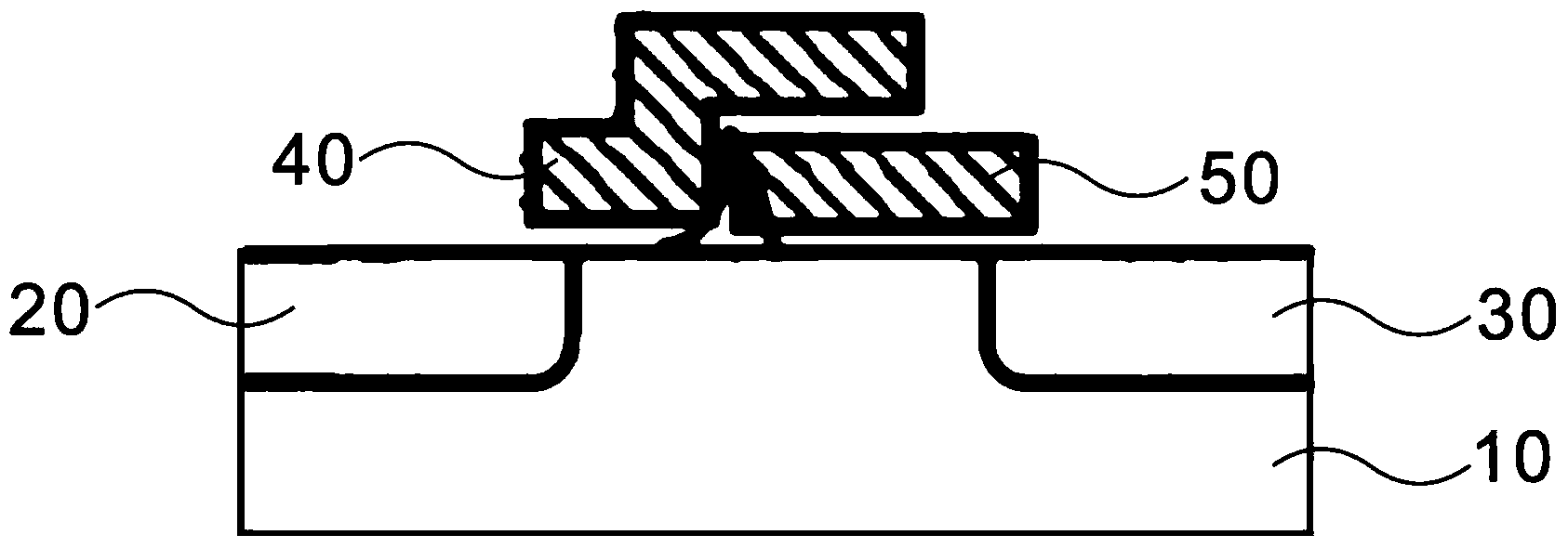
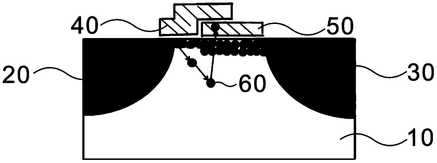
[0027] The semiconductor substrate 10 is a P-type substrate, the material of the control gate 40 and the floating gate 50 is polysilicon, and the material of the oxide layer is silicon dioxide, wherein the control gate 40 has a length of 10 nm and a height of 90 nm, and the floating gate 50 has a height of 70 nm and a length of 40 nm. , the thickness of the oxide layer is 2nm; during the programming operation, the threshold voltage Vth of the flash memory device is 0.7V, the applied voltage to the drain terminal 30 is 2V, the applied voltage to the floating gate 50 is 3V, and the applied voltage to the control gate 40 is The voltage is 0.7V, the voltage applied to the semiconductor substrate 10 is 1.5V, and the voltage applied to the source terminal 20 is 0V.

Example Embodiment

[0028] Embodiment two

[0029] The semiconductor substrate 10 is a P-type substrate, the material of the control gate 40 and the floating gate 50 is polysilicon, and the material of the oxide layer is silicon dioxide, wherein the control gate 40 has a length of 10 nm and a height of 90 nm, and the floating gate 50 has a height of 70 nm and a length of 40 nm. , the thickness of the oxide layer is 3.5nm; during the programming operation, the threshold voltage Vth of the flash memory device is 0.7V, the applied voltage to the drain terminal 30 is 3V, the applied voltage to the floating gate 50 is 2V, and the control gate 40 The applied voltage is 1V, the applied voltage of the semiconductor substrate 10 is 1V, and the source terminal 20 is applied with a voltage of 0V.

[0030] The manufacturing method of the flash memory device provided by the present invention is an existing manufacturing method of the flash memory device, which can be obtained by those skilled in the art throu...


PUM

PropertyMeasurementUnit
Thicknessaaaaaaaaaa
Thicknessaaaaaaaaaa
Thicknessaaaaaaaaaa

Abstract

The invention provides a programming method for a flash memory device. A flash memory comprises a semiconductor substrate, wherein a source end and a drain end which are arranged in a spaced manner are arranged on the semiconductor substrate; a control gate and a floating gate are arranged above a gap between the source end and the drain end. The programming method for the flash memory device comprises the following steps: when programming operation is performed, respectively applying voltages to the drain end, the floating gate, the control gate and the semiconductor substrate, wherein the range of the voltages applied to the drain end and the floating gate is 2 V to 3 V; the range of the voltages applied to the control gate is 0.7 to 1.0 V; the range of the voltage applied to the semiconductor substrate is 1 V to 1.5 V. According to the method provided by the invention, a channel punch-through effect caused by applying the high voltage to the drain end can be avoided, the critical dimensions of breakdown gate-floating gate flash memories are effectively shortened, and the unit density of an NOR-type or NAND-type flash memory array which takes the breakdown gate-floating gate flash memories as unit devices is increased, so that the storage capacity and the density of the flash memory are improved, and the reliability of the device is improved.

Description

technical field [0001] The invention relates to the field of semiconductor integrated circuits and its manufacture, in particular to a programming method of a flash memory device. Background technique [0002] In semiconductor storage devices, flash memory is a non-volatile memory, and belongs to erasable programmable read-only memory (EPROM). Generally, a flash memory has two gates (a floating gate and a control gate), wherein the floating gate is used to store charges, and the control gate is used to control data input and output. The position of the floating gate is below the control gate, and it is in a floating state because it is not connected to the external circuit. The control gate is usually connected to a word line. The advantage of flash memory is that it can erase the entire memory block, and the erasing speed is fast, only about 1 to 2 seconds. Generally speaking, flash memory has a split gate structure or a stacked gate structure or a combination of the two...

Claims


Application Information

Patent Timeline
IPC IPC(8): G11C16/10G11C16/34
Inventor 顾经纶王伟
Owner SHANGHAI HUALI MICROELECTRONICS CORP
Why Eureka
Try Eureka