Integration of 1T1R CBRAM memory cells

a memory cell and cbram technology, applied in the field of memory cell array or memory cell field, can solve the problems of no optimum solution, limited read cycle, high energy consumption of dram chip, etc., and achieve the effect of restricting the diffusion region of solid body electrolyte material and restricting spa

Inactive Publication Date: 2006-06-29
INFINEON TECH AG
View PDF11 Cites 33 Cited by
  • Summary
  • Abstract
  • Description
  • Claims
  • Application Information

AI Technical Summary

Benefits of technology

[0026] The principle of the present invention is based on the providing and the use of a common top electrode or plate line, respectively, for a plurality of CBRAM memory cells that are integrated or arranged in a memory cell array. To this end, this common top electrode is structured at the edge of the memory cell array or of the memory cell field, respectively, or at some other suitable position. The manufacturing of the common top electrode or plate line, respectively, is preferably performed by dry chemical or wet chemical methods, and is thus restricted in space.
[0027] For manufacturing the inventive memory cell array with integrated CBRAM memory cells, the CBRAM memory cell is placed on the so-called CC contact (“node contact”) or over the so-called CC contact, respectively, which is connected with the respective selection transistor in the silicon substrate via a co-called CA contact. In accordance with preferred embodiments of the inventive method there are suggested different integration approaches by which the active material (e.g. GeSe / Ag) of the solid body electrolyte memory cell is structured.
[0028] According to a preferred embodiment of the inventive method, the active solid body electrolyte material is filled into the back-etched CC contact and subsequently planarized. This process is preferably performed with the additional establishing of barrier layers so as to limit the diffusion region of the solid body electrolyte material.
[0029] To this end, the finished and planarized contact is, for instance, etched back by wet chemical etching by a particular degree so as to create the space required for the memory resistor. In addition, the memory cell array or the cell field, respectively, may be covered relative to the periphery by means of an uncritical lithography step. Subsequently, the ion conductor material (e.g. GeSe) and the reactive metal (e.g. Ag) may be deposited. Then, both the ion conductor material and the reactive metal are planarized by means of chemical mechanical polishing (CMP).
[0030] Alternatively, it is possible to first deposit and planarize the ion conductor material, and to subsequently commonly deposit planarly reactive metal and the plate electrode. This way it can be prevented that the reactive metal (Ag) is structured. At any rate, however, the plate electrode is structured after its deposition with a likewise uncritical lithography step at the edges of the memory cell array or the cell field, respectively, or at some other suitable position.
[0031] In accordance with a second preferred embodiment of the inventive method, a diffusion barrier, for instance, of SiN is applied conformely after the back-etching of the plug (and TiN liner), and subsequently the contact to the plug is re-established by means of anisotropic etching. This prevents a possible diffusing out of the active materials such as silver ions.

Problems solved by technology

The problem of the leaking currents existing with the DRAM memory concept, which result in a loss of charge or a loss of information, respectively, has so far been solved insufficiently only by the permanent refreshing of the stored charge, which results in a high energy consumption of the DRAM chip.
The flash memory concept underlies the problem of write and read cycles limited by barrier layers, wherein no optimum solution has been found yet, either, for the high switching voltages and the slow read and write cycles.
So far, there have only been known results from the manufacturing of individual cells in vertical or co-planar geometry, which are, however, less suited for highly dense memories.

Method used


Image

  • Integration of 1T1R CBRAM memory cells
  • Integration of 1T1R CBRAM memory cells
  • Integration of 1T1R CBRAM memory cells

Examples


Embodiment Construction

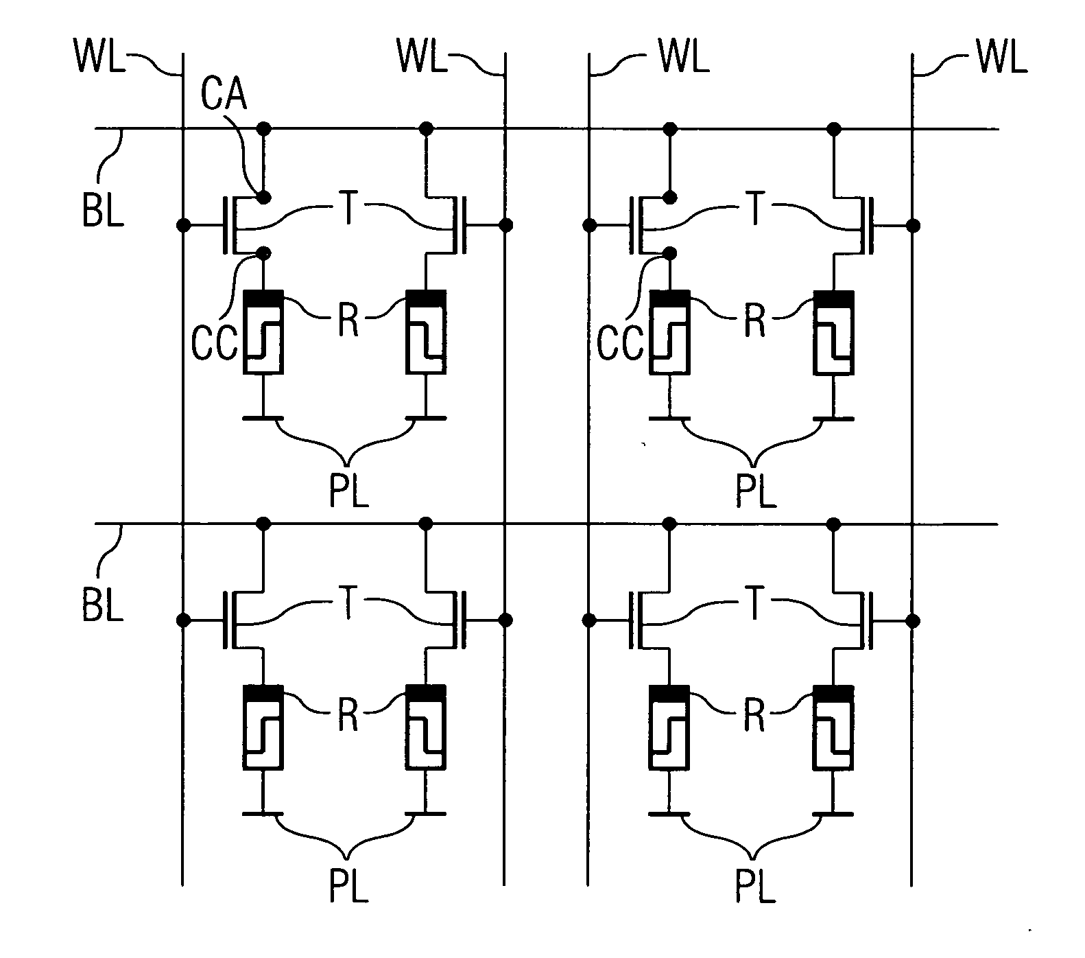
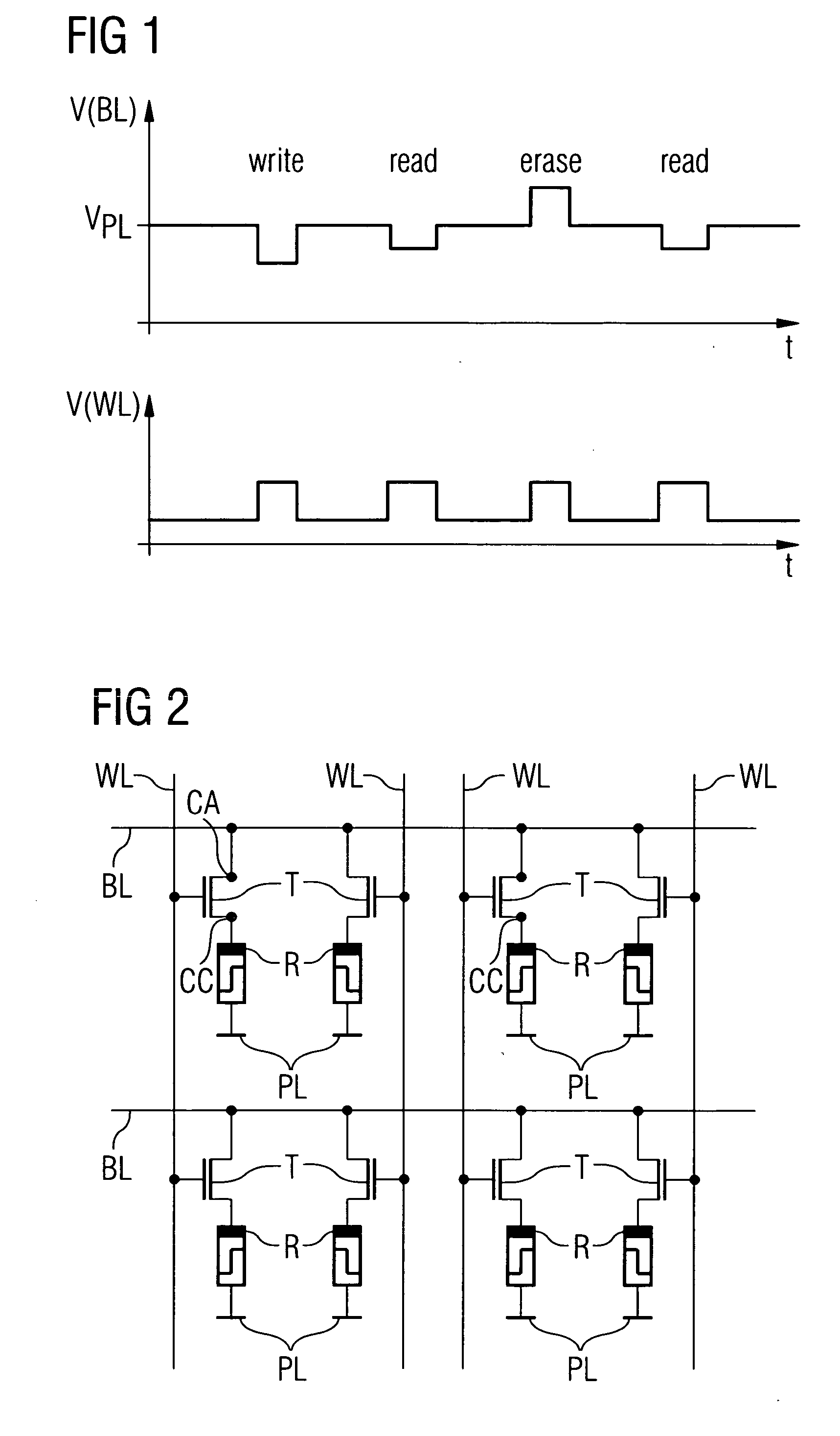
[0046]FIG. 1 shows respective diagrams for pulse triggering in the form of voltage pulses at the bit line V(BL) and at the word line V(WL) of a resistively switching solid body electrolyte memory cell. The diagrams each show a time sequence of a write pulse “write”, a read pulse “read”, an erase pulse “erase”, and a further read pulse “read” at the electrodes of the solid body electrolyte memory cell.

[0047] As described above, metal ions are diffused in a controlled manner from the anode into the ion conductor of the solid body electrolyte memory cell by applying bipolar voltage pulses at the electrodes of the solid body electrolyte memory cell. On applying a positive electric write voltage Uwrite>Uread at the electrodes of the solid body electrolyte memory cell, the metal cations diffuse from the anode under the influence of the external electric field through the ion conductor in the direction of the cathode, and dissolve in the ion conductor. The extent of the ion diffusion is c...


PUM


Abstract

A memory cell field with an integrated arrangement of solid body electrolyte memory cells, and in particular of CBRAM solid body electrolyte memory cells with 1T1R architecture, wherein the solid body electrolyte memory cells each comprise a layer stack that comprises at least a bottom and a top electroconductive, in particular metal layer and a layer of solid body electrolyte material or ion conductor material, respectively, positioned therebetween, and wherein each solid body electrolyte memory cell can be controlled via a word line, a bit line, and a plate line by means of a selection transistor, wherein at least a number of solid body electrolyte memory cells in the memory cell field have a common plate electrode or are connected to a common plate line, respectively.

Description

CLAIM FOR PRIORITY [0001] This application claims the benefit of priority to German Application No. 10 2004 061 548.9, filed in the German language on Dec. 21, 2004, the contents of which are hereby incorporated by reference. TECHNICAL FIELD OF THE INVENTION [0002] The invention relates to a memory cell array or a memory cell field, respectively, for the integration of resistively switching solid body electrolyte memory cells. The invention further relates to a method for manufacturing a memory cell field with an integrated arrangement of solid body electrolyte memory cells, and in particular of 1T1R CBRAM memory cells in minimum structure size. BACKGROUND OF THE INVENTION [0003] An integrated memory device usually comprises a cell field (array) consisting of a plurality of memory cells and a matrix of electroconductive supply lines which is composed of column and row supply lines or word and bit lines, respectively. With this type of memory arrays with so-called crosspoint architec...

Claims


Application Information

Patent Timeline
Patent Type & Authority Applications(United States)
IPC IPC(8): G11C11/00
CPCG11C13/0011G11C2213/79H01L45/1658H01L45/1675H01L45/1683H01L45/085H01L45/1233H01L45/142H01L45/143H01L27/2436H10B63/30H10N70/245H10N70/8822H10N70/8825H10N70/826H10N70/046H10N70/066H10N70/063
Inventor GRUNING VON SCHWERIN, ULRIKEHAPP, THOMASPINNOW, CAY-UWEROHR, THOMAS
Owner INFINEON TECH AG
Why Eureka
Try Eureka