Formation method of semiconductor structure and mask

A semiconductor and mask technology, applied in semiconductor devices, semiconductor/solid-state device manufacturing, electric solid-state devices, etc., can solve the problems of increasing the difficulty and complexity of integrated circuits, achieve small changes, low process complexity, and meet high density and highly integrated effects

Pending Publication Date: 2022-04-22
SEMICON MFG INT (SHANGHAI) CORP +1
View PDF0 Cites 0 Cited by
  • Summary
  • Abstract
  • Description
  • Claims
  • Application Information

AI Technical Summary

Problems solved by technology

[0003] During the development of integrated circuits, usually as the functional density (that is, the number of interconnection structures per chip) gradually increases, the geometric size (that is, the minimum component size that can be produced using process steps) also gradually decreases. Correspondingly increases the difficulty and complexity of integrated circuit manufacturing
[0004] At present, in the case of shrinking technology nodes, how to improve the matching degree between the pattern formed on the wafer and the target pattern has become a challenge

Method used


Image

  • Formation method of semiconductor structure and mask
  • Formation method of semiconductor structure and mask
  • Formation method of semiconductor structure and mask

Examples


Embodiment Construction

[0039] It can be known from the background art that how to improve the matching degree between the pattern formed on the wafer and the target pattern becomes a challenge in the case of shrinking technology nodes.

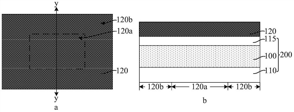
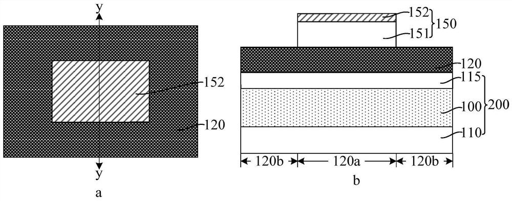
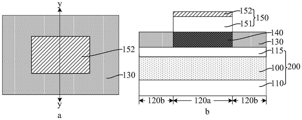
[0040] In order to solve the above technical problem, an embodiment of the present invention provides a method for forming a semiconductor structure, performing ion doping on the core material layer in the second region to form an anti-etching layer in the second region and a layer in the second region. The core layer of the first region, in the step of forming the first trench, in the second direction, part of the core material layer of the first region remains on both sides of the first trench, that is, In other words, the first region spans the first groove along the second direction, and then forms sidewalls on the sidewalls of the first groove, so that the sidewalls enclose the first groove, and after removing the core layer In the step, the formed second groov...


PUM


Abstract

The invention discloses a semiconductor structure forming method and a mask, and the method comprises the steps: providing a substrate which comprises a target layer; forming a core material layer on the substrate, wherein the core material layer comprises a first region and a second region surrounding the first region; ion doping is carried out on the core material layer of the second area, the etching resistance of the core material layer is improved, the core material layer located in the second area serves as an etching resistance layer, and the core material layer located in the first area serves as a core layer; forming a first groove penetrating through at least part of the core material layer in the first region along the first direction, and reserving part of the core material layer in the first region on two sides of the first groove in the second direction; a side wall is formed on the side wall of the first groove, so that a first groove is defined by the side wall; removing the core layer to form a second groove; and etching the target layer below the first groove and the second groove by taking the anti-etching layer and the side wall as masks to form a target pattern. The embodiment of the invention is beneficial to further compressing the pitch between the target patterns.

Description

technical field [0001] Embodiments of the present invention relate to the field of semiconductor manufacturing, and in particular, to a method for forming a semiconductor structure and a mask. Background technique [0002] With the rapid growth of the semiconductor integrated circuit (Integrated circuit, IC) industry, semiconductor technology continues to move towards smaller process nodes driven by Moore's Law, making integrated circuits smaller in size, higher in circuit precision, and development in the direction of higher complexity. [0003] During the development of integrated circuits, usually as the functional density (that is, the number of interconnection structures per chip) gradually increases, the geometric size (that is, the minimum component size that can be produced using process steps) also gradually decreases. Correspondingly increases the difficulty and complexity of integrated circuit manufacturing. [0004] At present, how to improve the matching degre...

Claims


Application Information

Patent Timeline
Patent Type & Authority Applications(China)
IPC IPC(8): H01L21/768
CPCH01L21/76816H01L2221/101H01L21/31144H01L21/0337H01L21/32155H01L21/32134H01L21/0332H01L21/3215H01L21/31155
Inventor 金吉松
Owner SEMICON MFG INT (SHANGHAI) CORP
Why Eureka
Try Eureka