Method for shortening analytic period of mfg. process

A technology of photoresist layer and material layer, which is applied in the field of shortening the analysis cycle of the process, can solve the problems that the process width of semiconductor elements cannot be reduced, and the efficiency of the process operation is limited, and the flexibility of the process operation is limited.

Inactive Publication Date: 2004-01-07
MACRONIX INT CO LTD
View PDF0 Cites 0 Cited by
  • Summary
  • Abstract
  • Description
  • Claims
  • Application Information

AI Technical Summary

Problems solved by technology

However, these materials exposed by deep ultraviolet light or off-axis light have their limitations, which cannot make the process width of semiconductor devices shrink smoothly, and limit the operating efficiency and flexibility of the process.

Method used


Image

  • Method for shortening analytic period of mfg. process
  • Method for shortening analytic period of mfg. process
  • Method for shortening analytic period of mfg. process

Examples


Embodiment Construction

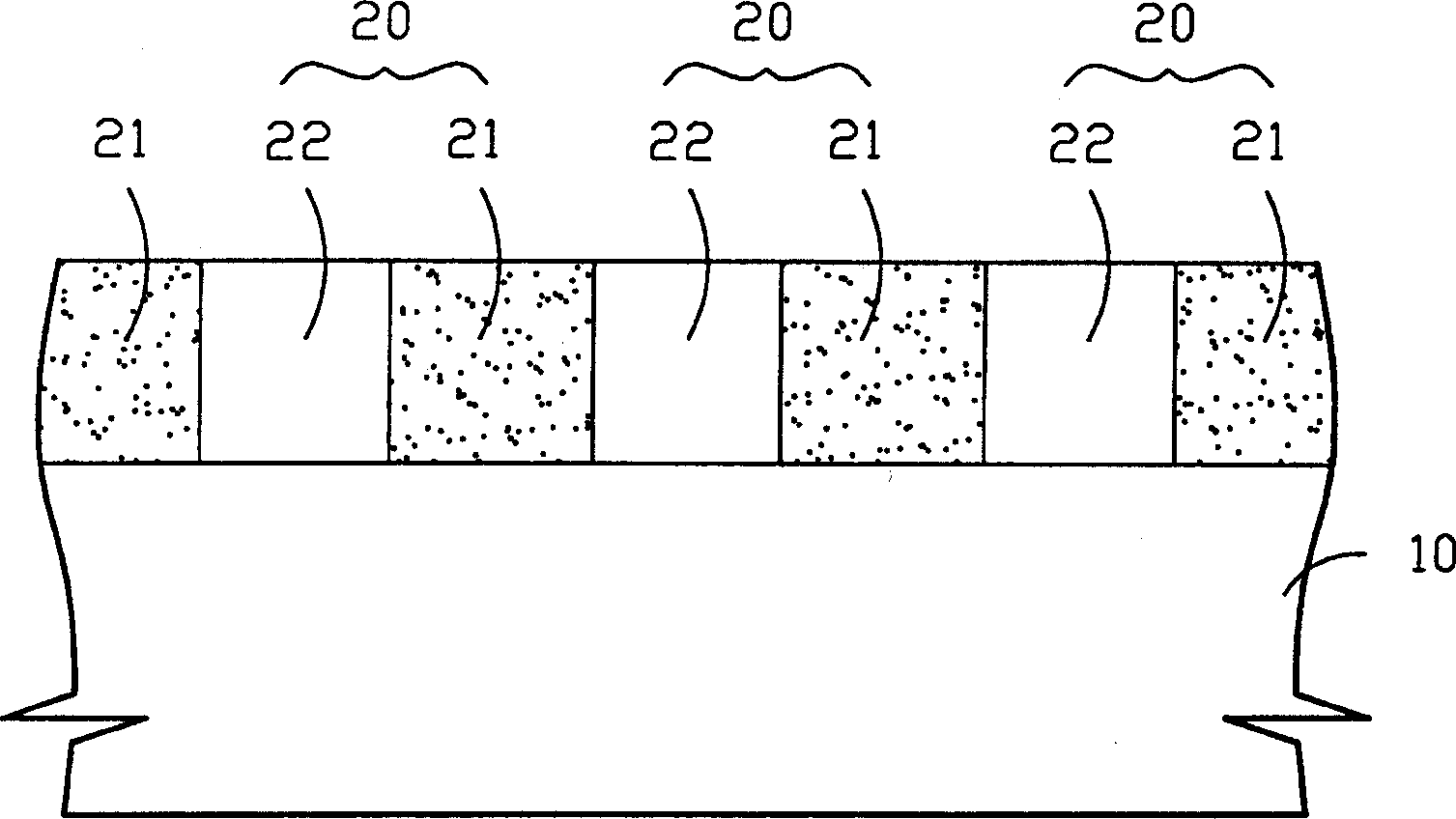
[0029] refer to Figure 4 As shown, this is a schematic diagram of forming a photoresist layer on a part of the substrate. Firstly, a wafer is provided, and the wafer includes a substrate 100 . Next, a first photoresist layer 200 is formed on the substrate 100 . The first photoresist layer 200 can be a photoresist layer exposed by deep ultraviolet light or a photoresist layer exposed by i-line light, but this does not limit the scope of the present invention. Usually, the first photoresist layer 200 is made of a photoresist layer exposed by deep ultraviolet light. Next, a photomask is used to carry out a first photolithography process, so as to completely transfer the pattern on the photomask to the first photoresist layer 200 . Next, part of the first photoresist layer 200 is removed to form the first photoresist layer 200 on part of the substrate 100 . In the lithography process, the light source used by the exposure machine can be any type of light source, such as off-a...


PUM


Abstract

This invention relates to a method for reducing an analytical period of a process including: using a light mask to form a first light resistance layer on part of a basic material and a first material layer on sidewall of the layer, removing the first layer to form a first material layer on part of the basic material at the first stage, carrying out a second process to form a second light resistance layer on the first material layer sidewall, removing the first light resistance layer to form a ditch on the basic material and form a second material layer on sidewall of the ditch, finally, removing the second light resistance layer to form a complex layer of the first and second material layers, so, the first and second layer and contacted together.

Description

(1) Technical field [0001] The present invention relates to a method for reducing the width of a process, in particular to a method for reducing the analysis period of a process. (2) Background technology [0002] When the density of integrated circuits (ICs) continues to expand, in order to keep the chip area the same or even reduce it, and to continuously reduce the unit cost of the circuit, the only way is to continuously reduce the circuit design specification (design rule) ). When reducing the size, the biggest bottleneck encountered is the yellow light lithography technology. Unless yellow light lithography imaging can be gradually reduced, the development of integrated circuit technology will suffer the fate of stagnation. [0003] Photolithography in the integrated circuit manufacturing process is to convert a large number of electronic components and circuits into a tiny chip layer by layer, each layer has a mask, relying on the principle of optical imaging, The ...

Claims


Application Information

Patent Timeline
Patent Type & Authority Applications(China)
IPC IPC(8): G03F7/00H01L21/027
Inventor 張慶裕鍾維民
Owner MACRONIX INT CO LTD
Why Eureka
Try Eureka