Manufacturing method of through hole

A manufacturing method and photoresist technology, which is applied in semiconductor/solid-state device manufacturing, electrical components, circuits, etc., can solve the problems of photoresist consumption, photoresist thickness, and adverse effects of opening morphology, and achieve the key to shrinking The effect of less size and thickness consumption and good shape

Inactive Publication Date: 2021-04-09
HUA HONG SEMICON WUXI LTD +1
View PDF4 Cites 1 Cited by
  • Summary
  • Abstract
  • Description
  • Claims
  • Application Information

AI Technical Summary

Problems solved by technology

In addition, during the etching process of the interlayer film, the photoresist will be consumed. When the thickness of the photoresist is not enough, it will adversely affect the opening morphology of the through hole formed by etching.
Therefore, in the existing method, the thickness of the photoresist is not easy to control, and the photoresist is too thick, which is not conducive to the reduction of the critical dimension of the opening of the through hole; and the photoresist is too thin, which is not conducive to the interlayer film etching process. Controlling the opening morphology of vias; this makes it impossible for existing methods to obtain small-sized vias with high aspect ratios

Method used


Image

  • Manufacturing method of through hole
  • Manufacturing method of through hole
  • Manufacturing method of through hole

Examples


Embodiment Construction

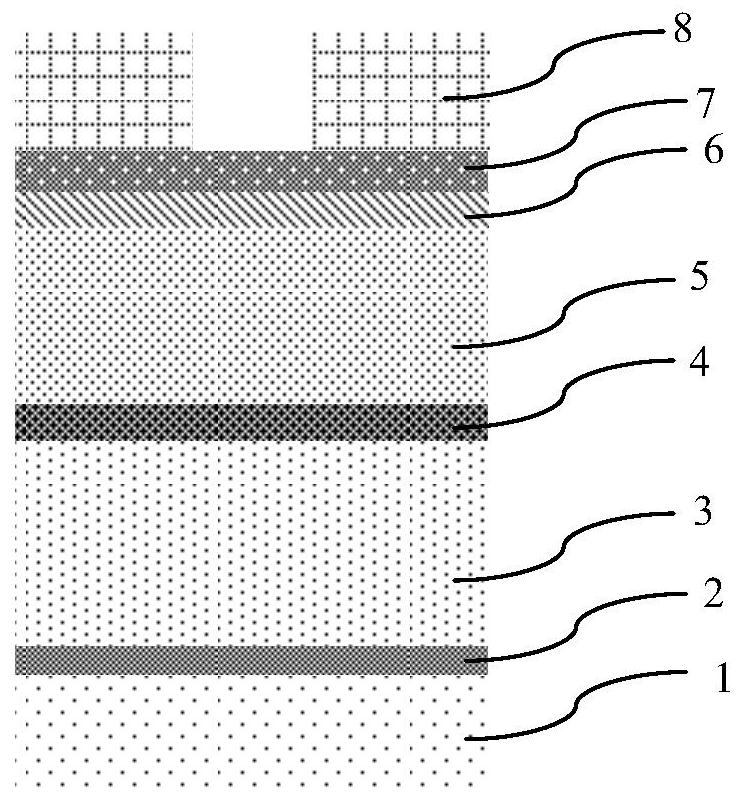
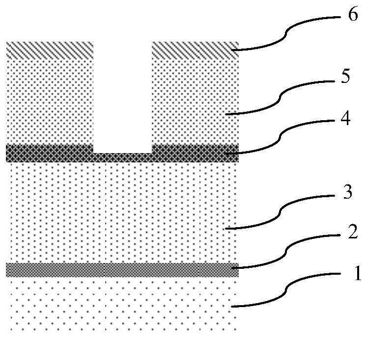
[0034] Such as figure 1 Shown is the flow chart of the manufacturing method of the through hole of the embodiment of the present invention; Figure 2A to Figure 2D As shown, it is a schematic diagram of the device structure in each step of the embodiment of the present invention; the manufacturing method of the through hole in the embodiment of the present invention includes the following steps:

[0035] Step 1, such as Figure 2A As shown, an underlying structure with an interlayer film 3 formed on the surface is provided, and a dielectric antireflection coating 4 is formed on the surface of the interlayer film 3 .

[0036] The underlying structure includes multiple underlying interlayer films and underlying metal layers formed on the semiconductor substrate, and the underlying metal layers are isolated by the corresponding underlying interlayer films. Figure 2A , the topmost layer of the underlying metal layer 1 is shown. Subsequently, in step six, the opening of the thr...


PUM


Abstract

The invention discloses a manufacturing method of a through hole. The manufacturing method comprises the following steps: 1, forming a DARC layer on the surface of an interlayer film; 2, forming a nitrogen-free doped carbon coating on the surface of the DARC layer; 3, forming a low-temperature oxide layer on the surface of the nitrogen-free doped carbon coating, and superposing the nitrogen-free doped carbon coating and the low-temperature oxide layer to form a hard mask layer; 4, carrying out photoetching to form a photoresist pattern, and opening a forming area of the through hole; 5, performing first etching on the hard mask layer in the forming area of the through hole by taking the photoresist pattern as a mask; and 6, etching the DARC layer and the interlayer film for the second time in sequence by taking the hard mask layer as a mask to form an opening of the through hole. According to the invention, the through hole with small size and high depth-to-width ratio can be obtained.

Description

technical field [0001] The invention relates to a method for manufacturing a semiconductor integrated circuit, in particular to a method for manufacturing a through hole. Background technique [0002] In the manufacture of semiconductor integrated circuits, it is first necessary to form semiconductor device structures such as various doped regions of semiconductor devices such as source and drain regions and gate structures such as polysilicon gates on a semiconductor substrate such as a silicon substrate, and then form metal interconnections The structure leads out each doped region of the semiconductor device formed on the semiconductor substrate. [0003] In the metal interconnection structure, it includes multiple metal layers, an interlayer film located between each of the metal layers, and a through hole passing through the interlayer film to realize the connection of each of the metal layers. [0004] With the continuous reduction of process nodes, the critical dimen...

Claims


Application Information

Patent Timeline
Patent Type & Authority Applications(China)
IPC IPC(8): H01L21/768
CPCH01L21/76804H01L21/76813H01L21/76816
Inventor 姚道州孟艳秋
Owner HUA HONG SEMICON WUXI LTD
Why Eureka
Try Eureka