Trench type field effect transistor structure and preparation method thereof

A field-effect transistor, trench-type technology, used in transistors, semiconductor/solid-state device manufacturing, semiconductor devices, etc., can solve the problems of poor electrical connection in the body region, low EAS capability, etc., to improve EAS capability, The effect of improving doping uniformity and increasing cell density

Active Publication Date: 2021-03-19
CHINA RESOURCES MICROELECTRONICS (CHONGQING) CO LTD
View PDF10 Cites 0 Cited by
  • Summary
  • Abstract
  • Description
  • Claims
  • Application Information

AI Technical Summary

Problems solved by technology

[0005] In view of the shortcomings of the prior art described above, the purpose of the present invention is to provide a trench type field effect transistor structure and its preparation method, which are used to solve the problem of poor electrical connection and EAS capability of the body region in the prior art. low problem

Method used


Image

  • Trench type field effect transistor structure and preparation method thereof
  • Trench type field effect transistor structure and preparation method thereof
  • Trench type field effect transistor structure and preparation method thereof

Examples


Embodiment 1

[0081] Such as Figure 1-14 As shown, the present invention provides a method for preparing a trench field effect transistor structure, the preparation method of the trench field effect structure at least includes the following steps:

[0082] 1) providing a substrate of a first doping type, and forming an epitaxial layer of the first doping type on the substrate;

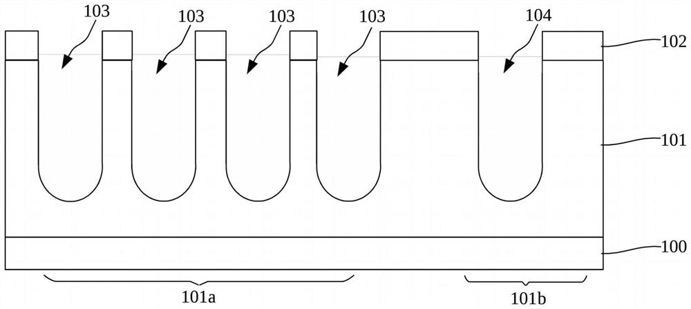
[0083] 2) Forming a trench mask on the epitaxial layer, and forming a plurality of device trenches arranged in parallel at intervals in the epitaxial layer based on the trench mask, and retaining the rest of the trench mask ;

[0084] 3) forming a gate oxide layer on the sidewall and bottom of the device trench, and forming a first conductive layer on the surface of the gate oxide layer, the first conductive layer fills the device trench and extends to the In the trench mask;

[0085] 4) performing ion implantation on the structure obtained in step 3), so as to form a body region of the second doping type in the...

Embodiment 2

[0129] Such as Figure 14 shown, see Figure 1-13 , the present invention also provides a trench type field effect transistor structure, the trench type field effect structure at least includes:

[0130] a substrate 100 of a first doping type;

[0131] The epitaxial layer 102 of the first doping type, the epitaxial layer 102 is formed on the substrate 100;

[0132] a plurality of device trenches 103 arranged in parallel at intervals, the device trenches 103 are formed in the epitaxial layer 102;

[0133] a gate oxide layer 106 formed on the sidewall and bottom of the device trench 103;

[0134] a gate structure layer 111 formed on the surface of the gate oxide layer 106, and the upper surface of the gate structure layer 111 is lower than the upper surface of the gate oxide layer 106;

[0135] A body region 110 of a second doping type, the body region 110 is formed between adjacent device trenches 103 and the depth of the body region 110 does not exceed the depth of the dev...


PUM


Abstract

The invention provides a trench type field effect transistor structure and a preparation method thereof. The preparation method comprises the steps: providing a substrate of a first doping type, forming an epitaxial layer of the first doping type, forming a trench mask, forming a device trench, forming a gate oxide layer, forming a first conductive layer, forming a body region of a second doping type, forming a source injection region, forming a source electrode of the first doping type based on the trench mask, forming an insulating dielectric layer, enabling the upper surface of the insulating dielectric layer, the upper surface of the gate oxide layer, the upper surface of the source electrode and the upper surface of the body region to be flush, and forming a source electrode. According to the invention, the advantages of a self-alignment process are retained, cell density is effectively increased, a transistor structure and process are improved, the effective electrical extractionof the source electrode and the body region is realized, the key size of a cell is reduced, the electrical extraction mode of the source electrode and the body region is changed while the cell density is improved, the EAS capability of a device is improved, the doping uniformity of the body region is improved, and an extra body region leading-out region does not need to be prepared.

Description

technical field [0001] The invention relates to the technical field of integrated circuit design and manufacture, in particular to a trench type field effect transistor structure and a preparation method thereof. Background technique [0002] Compared with planar power devices, deep trench power devices have the characteristics of high integration, low on-resistance, fast switching speed, and low switching loss. They have been widely used in power conversion and control. [0003] For low-voltage deep trench power devices, the channel resistance Rchannel accounts for about 30% to 40%, and the substrate resistance Rsub accounts for about 40% to 50%. The channel resistance Rchannel is determined by the channel density. In order to reduce the conduction To realize the extremely low on-state resistance of metal-oxide-semiconductor field-effect transistors (Metal-Oxide-Semiconductor Field-Effect Transistor, MOSFET), requires metal-oxide-semiconductor field-effect transistors to be...

Claims


Application Information

Patent Timeline
Patent Type & Authority Applications(China)
IPC IPC(8): H01L21/8234H01L21/28H01L27/088H01L29/417H01L29/423
CPCH01L21/823418H01L21/823462H01L21/823437H01L27/088H01L29/4236H01L29/41725H01L29/401
Inventor 陈茜
Owner CHINA RESOURCES MICROELECTRONICS (CHONGQING) CO LTD
Why Eureka
Try Eureka