Public voltage compensation circuit and method, array substrate and display device

A common voltage, compensation circuit technology, applied in static indicators, instruments, etc., can solve problems such as crosstalk, picture jitter, affecting the display quality of liquid crystal displays and organic electroluminescence displays

Active Publication Date: 2014-12-17
CHONGQING BOE OPTOELECTRONICS +1
View PDF6 Cites 22 Cited by
  • Summary
  • Abstract
  • Description
  • Claims
  • Application Information

AI Technical Summary

Problems solved by technology

[0004] In existing liquid crystal displays and organic electroluminescent displays, the common voltage applied to the common electrode line by the common voltage generation circuit is easily affected by other voltages and appears to rise or fall, which will lead to liquid crystal displays and organic electroluminescent displays. The picture displayed by the light-emitting display has problems such as jitter, afterimage, abnormal display grayscale, and crosstalk, which affect the display quality of liquid crystal displays and organic electroluminescent displays.

Method used


Image

  • Public voltage compensation circuit and method, array substrate and display device
  • Public voltage compensation circuit and method, array substrate and display device
  • Public voltage compensation circuit and method, array substrate and display device

Examples


example 1

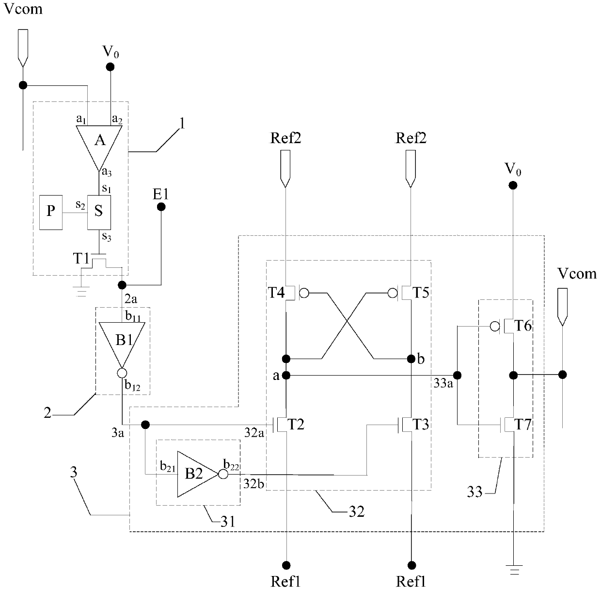
[0077] Example 1: if image 3 As shown, the control power supply P controls the sampler S to turn on, and the sampler S samples the comparison result of the common voltage and the reference voltage obtained by the comparator A:

[0078] When the difference between the common voltage and the reference voltage is greater than or equal to the preset threshold, the comparator A inputs a high-level signal to the gate of the first switching transistor T1 through the sampler S, so that the first switching transistor T1 is in a conducting state, so that the input terminal b of the first inverter B1 11 and the port E1 for inputting the first level signal is grounded; the gate of the first inverter B1 to the gate of the second switching transistor T2 and the input terminal b of the second inverter B2 21 output the second level signal, the second inverter B2 converts the second level signal into a zero-voltage signal and sends it to the gate of the third switching transistor T3, the sec...

example 2

[0080] Example 2: if Figure 4 As shown, the control power supply P controls the sampler S to turn on, and the sampler S samples the comparison result of the common voltage and the reference voltage obtained by the comparator A:

[0081] When the difference between the common voltage and the reference voltage is greater than or equal to the preset threshold, the comparator A inputs a high-level signal to the gate of the first switching transistor T1 through the sampler S, so that the first switching transistor T1 is in a conducting state, so that the input terminal b of the first inverter B1 11 and the port E1 for inputting the first level signal is grounded; the gate of the first inverter B1 to the gate of the second switching transistor T2 and the input terminal b of the second inverter B2 21 output the second level signal, the second inverter B2 converts the second level signal into a zero-voltage signal and sends it to the gate of the third switching transistor T3, the se...

example 3

[0083] Example 3: If Figure 5 As shown, the control power supply P controls the sampler S to turn on, and the sampler S samples the comparison result of the common voltage and the reference voltage obtained by the comparator A:

[0084] When the difference between the common voltage and the reference voltage is greater than or equal to the preset threshold, the comparator A inputs a high-level signal to the gate of the first switching transistor T1 through the sampler S, so that the first switching transistor T1 is in a conducting state, so that the input terminal b of the first inverter B1 11 and the port E1 for inputting the first level signal is grounded; the gate of the first inverter B1 to the gate of the second switching transistor T2 and the input terminal b of the second inverter B2 21 output the second level signal, the second inverter B2 converts the second level signal into a zero-voltage signal and sends it to the gate of the third switching transistor T3, the se...


PUM


Abstract

The invention discloses a public voltage compensation circuit and method, an array substrate and a display device. When the difference between the public voltage on a pubic electrode line and reference voltage is large, a comparing module outputs a zero voltage signal to a reversing module, the reversing module outputs a second level signal to a voltage adjusting module, the voltage adjusting module outputs the reference voltage to the public electrode line, and the public voltage compensation circuit compensates the public voltage on the public electrode line to allow the public voltage to be equal to the reference voltage; when the difference between the public voltage on the pubic electrode line and reference voltage is small, the comparing module outputs a first level signal to the reversing module, the reversing module outputs a zero voltage signal to the voltage adjusting module, the voltage adjusting module outputs the zero voltage signal to the public electrode line, and the public voltage compensation circuit does not compensates the public voltage on the public electrode line. By the public voltage compensation circuit and method, the public voltage on the public electrode line can be stabilized, and display frame abnormity of the display panel can be avoided.

Description

technical field [0001] The present invention relates to the field of display technology, in particular to a common voltage compensation circuit, a compensation method thereof, an array substrate and a display device. Background technique [0002] Among existing display devices, organic electroluminescence display (OLED, Organic Light Emitting Diode) has the advantages of simple preparation process, low cost, high luminous efficiency and easy formation of flexible structure; liquid crystal display (LCD, Liquid Crystal Display) has It has the advantages of low power consumption, high display quality, no electromagnetic radiation and wide application range. Organic electroluminescent displays and liquid crystal displays are relatively important display devices at present. [0003] Apply voltage to the pixel electrode and common electrode in the liquid crystal display, the electric field formed between the pixel electrode and the common electrode controls the rotation of liquid...

Claims


Application Information

Patent Timeline
Patent Type & Authority Applications(China)
IPC IPC(8): G09G3/32G09G3/36G09G3/3208
CPCG09G3/3208G09G3/3655G09G2330/12G09G3/3614G09G2330/028G09G3/3225
Inventor 许益祯
Owner CHONGQING BOE OPTOELECTRONICS
Why Eureka
Try Eureka