Array substrate and display panel

A technology for array substrates and display areas, applied in static indicators, nonlinear optics, instruments, etc., can solve the problem that the width of the frame cannot be further reduced, and achieve the effect of reducing the width and realizing a narrow frame

Active Publication Date: 2014-12-24
BOE TECH GRP CO LTD
View PDF5 Cites 16 Cited by
  • Summary
  • Abstract
  • Description
  • Claims
  • Application Information

AI Technical Summary

Problems solved by technology

[0004] In the above-mentioned array substrate 1, since the gate driving circuit 4 and the signal line 5 are arranged on the edge region 3, the edge region 3 needs to have a certain width, thus limiting the further reduction of the width of the edge region 3, so that in The width of the bezel cannot be further reduced in the liquid crystal display device

Method used


Image

  • Array substrate and display panel
  • Array substrate and display panel
  • Array substrate and display panel

Examples


Embodiment Construction

[0029] Specific embodiments of the present invention will be described in detail below in conjunction with the accompanying drawings. It should be understood that the specific embodiments described here are only used to illustrate and explain the present invention, and are not intended to limit the present invention.

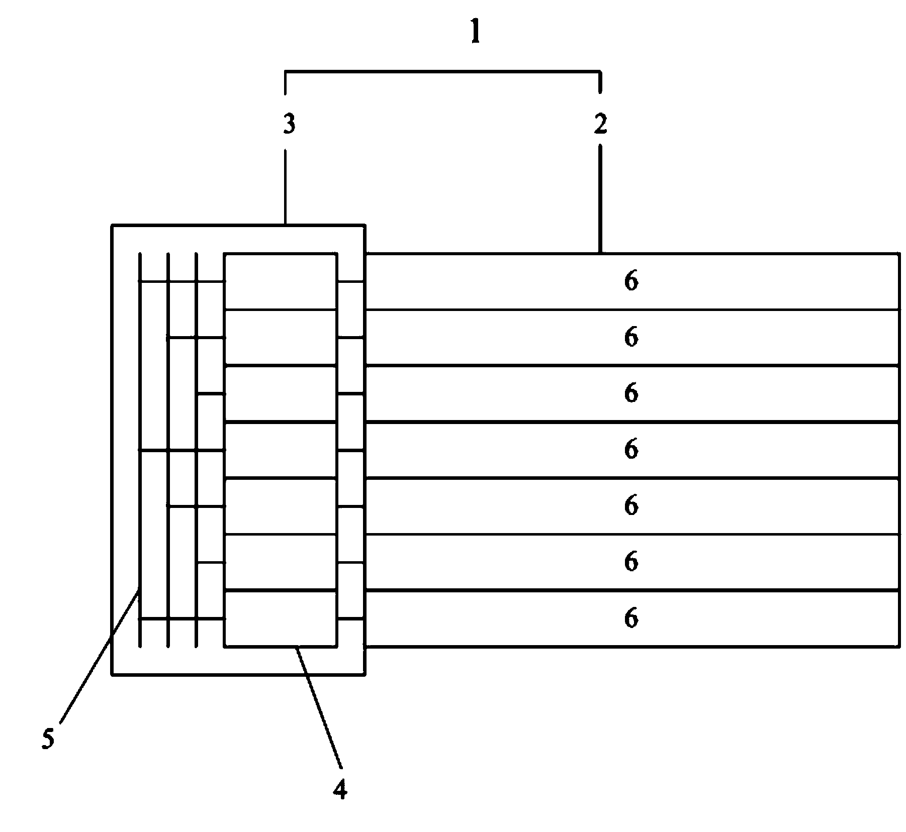
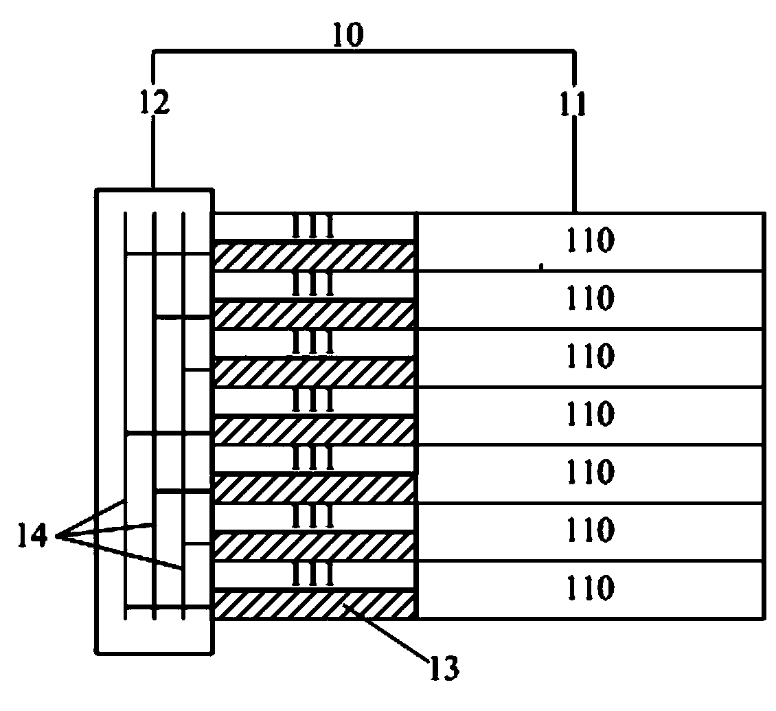
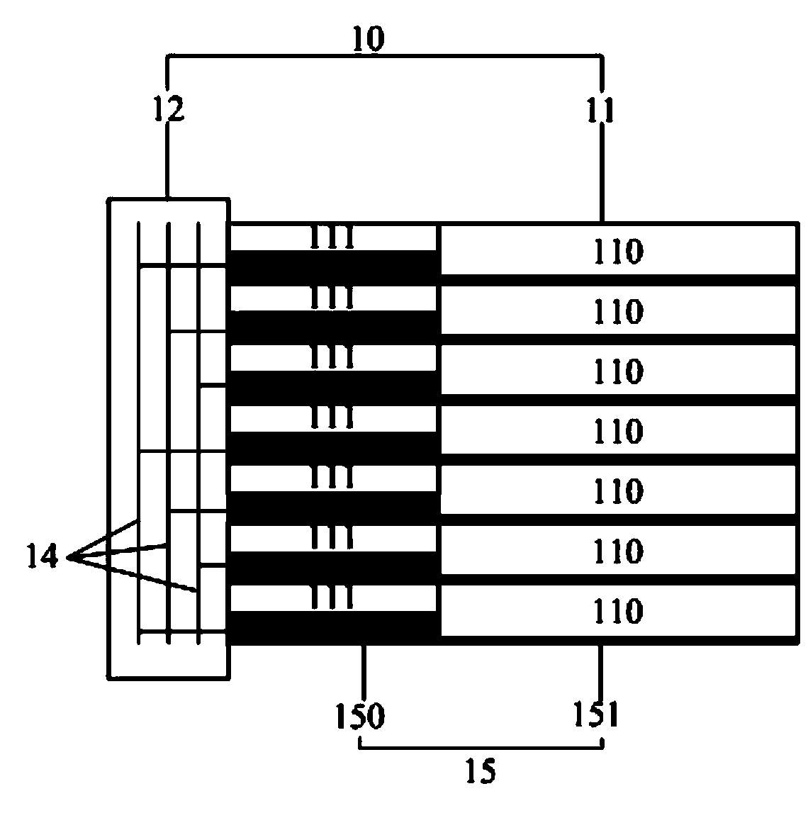
[0030] figure 2 It is a schematic diagram of the array substrate provided by the first embodiment of the present invention. Such as figure 2 As shown, the surface of the array substrate 10 includes an active display area (Active Area) 11 and an edge area 12 . A plurality of first pixels 110 are arranged in the effective display area 11, and the plurality of first pixels 110 are sequentially arranged along the lateral direction and the longitudinal direction of the array substrate 10, that is, along the lateral direction of the array substrate 10, the plurality of first pixels 110 can be divided into multiple rows , along the longitudinal direction of the ar...


PUM


Abstract

The invention relates to an array substrate and a display panel. The array substrate surface comprises an effective display area, and a plurality of first pixels are arranged in the effective display area. A grid drive circuit is arranged on the array substrate and arranged in the effective display area. The grid drive circuit comprises a plurality of levels of shifting register units arranged in the longitudinal direction of the array substrate at intervals, and a second pixel is arranged between every two adjacent levels of shifting register units. The grid drive circuit of the array substrate is arranged in the effective display area of the array substrate, the width of the edge area, on one side or the edge areas on the two sides of the effective display area, of the array substrate can be reduced, and a narrow frame can be obtained. In addition, the second pixels are arranged between every two adjacent levels of shifting register units, and therefore the area, in which the grid drive circuit is located, in the effective display area can still be used for display.

Description

technical field [0001] The present invention relates to the technical field of liquid crystal display, in particular to an array substrate and a display panel. Background technique [0002] In the preparation process of the array substrate of the liquid crystal display device, the gate driver circuit (Gate-driver IC) can be prepared on the array substrate (Array) through an etching process, that is, GOA (Gate-driver On Array), which can reduce The space occupied by the gate driving circuit can reduce the width of the frame of the screen, which is helpful to realize the narrow frame of the liquid crystal display panel. [0003] figure 1 It is a schematic diagram of an existing array substrate provided with a gate driving circuit. Such as figure 1 As shown, the array substrate 1 includes an active display area (Active Area) 2 and edge areas 3 located on both sides of the active display area. Wherein, multiple rows of pixels 6 are arranged on the effective display area 2 fo...

Claims


Application Information

Patent Timeline
Patent Type & Authority Applications(China)
IPC IPC(8): G09G3/36G02F1/133G02F1/1362
Inventor 姚星林允植韩承佑
Owner BOE TECH GRP CO LTD
Why Eureka
Try Eureka