Supercharge Your Innovation With Domain-Expert AI Agents!

PMOLED (passive matrix organic light emitting diode) array substrate as well as manufacturing method, display device and mask plate thereof

A technology of array substrates and mask plates, which is applied in photolithographic process exposure devices, semiconductor/solid-state device manufacturing, microlithography exposure equipment, etc., can solve the problems of large number of mask plates and high production costs, and achieve simplified manufacturing processes and production The effect of cost reduction and production cost reduction

Active Publication Date: 2014-12-24
BOE TECH GRP CO LTD
View PDF4 Cites 4 Cited by
  • Summary
  • Abstract
  • Description
  • Claims
  • Application Information

AI Technical Summary

Problems solved by technology

[0005] The disadvantage of the existing technology is that the number of masks used in the production process of the PMOLED array substrate is relatively large, and the production cost is relatively high.

Method used


Image

  • PMOLED (passive matrix organic light emitting diode) array substrate as well as manufacturing method, display device and mask plate thereof
  • PMOLED (passive matrix organic light emitting diode) array substrate as well as manufacturing method, display device and mask plate thereof
  • PMOLED (passive matrix organic light emitting diode) array substrate as well as manufacturing method, display device and mask plate thereof

Examples


Embodiment Construction

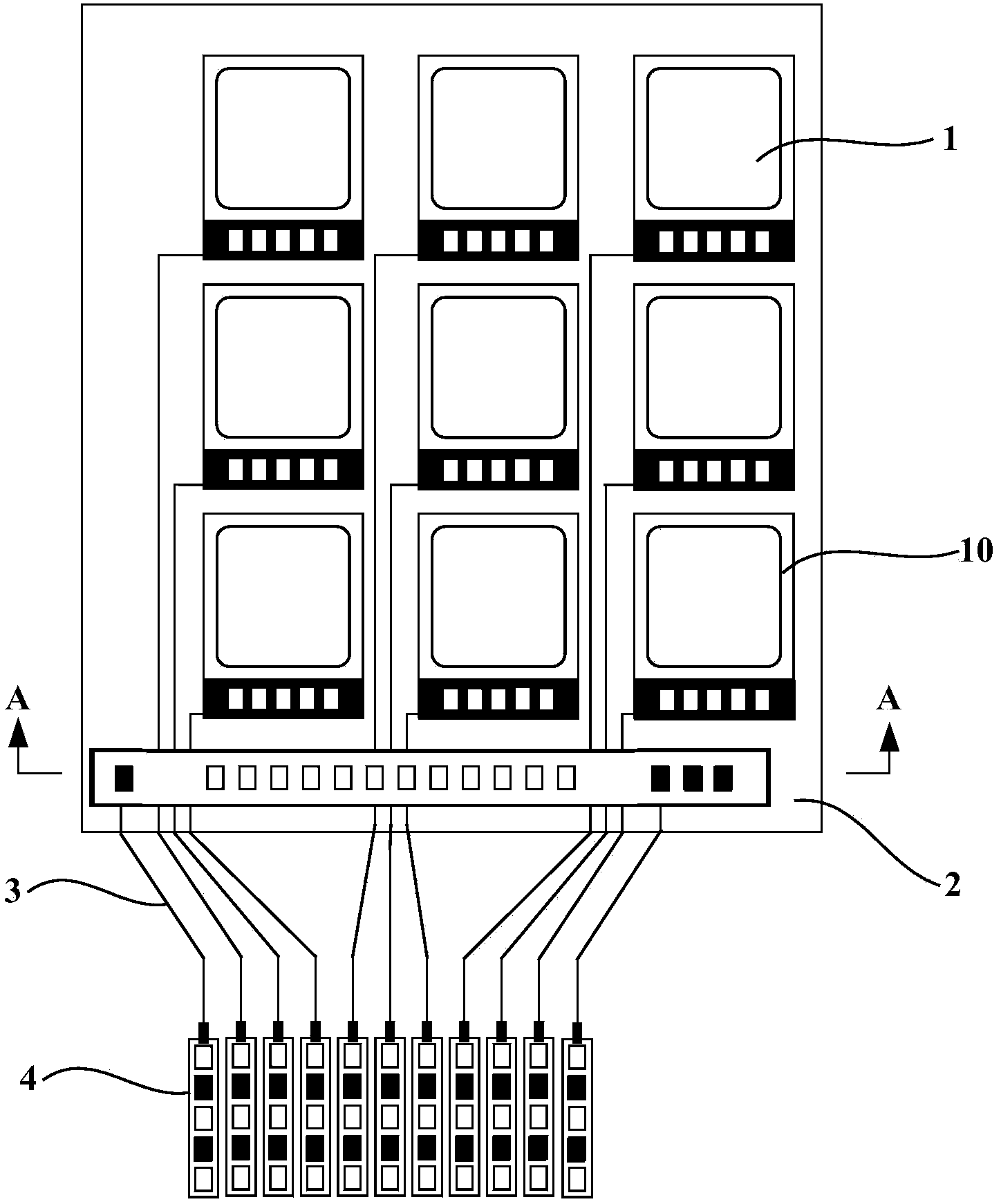
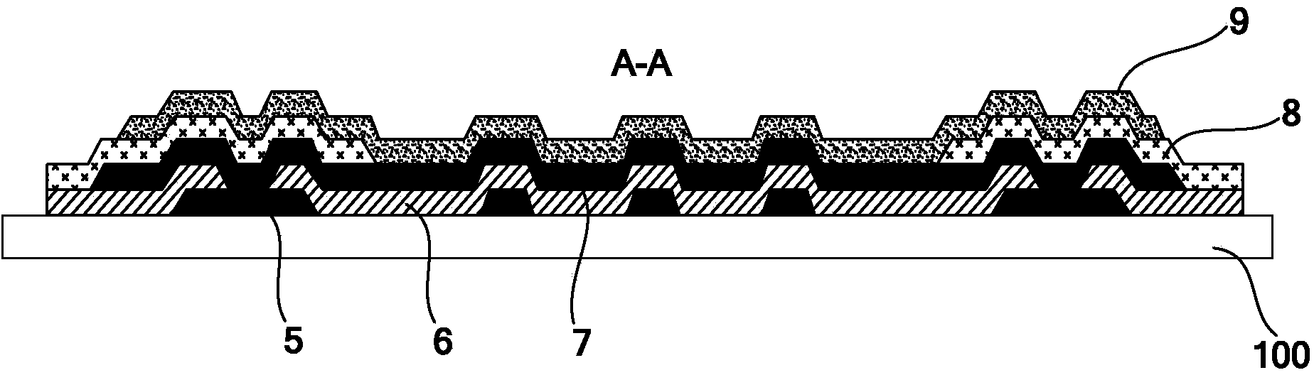
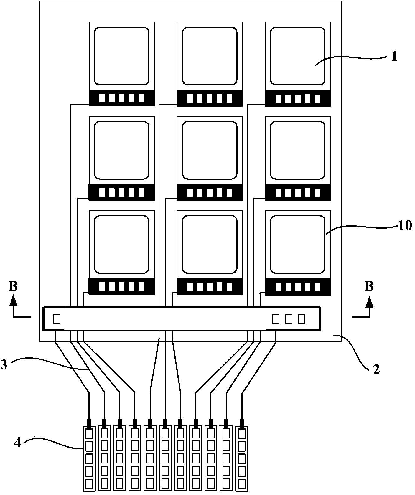
[0053] In order to reduce the number of masks used and reduce production costs, embodiments of the present invention provide a passive matrix OLED array substrate, a manufacturing method thereof, a display device, and a mask. In the technical solution of the present invention, the transparent conductive layer is located on the second metal layer, no insulating layer is provided between the transparent conductive layer and the second metal layer, and the transparent conductive layer and the second metal layer can be formed by using the same mask, Compared with the prior art, the number of masks used is reduced, the production cost is greatly reduced, and the manufacturing process is simplified.

[0054]In order to make the purpose, technical solution and advantages of the present invention clearer, the following examples are given to further describe the present invention in detail.

[0055] Such as image 3 with Figure 4 As shown, the passive matrix organic light emitting d...


PUM


Abstract

The invention relates to the field of display and discloses a PMOLED array substrate as well as a manufacturing method, a display device and a mask plate thereof. The array substrate comprises a first metal layer, an insulating layer, a second metal layer and a transparent conducting layer, wherein the first metal layer is located on a substrate base plate and comprises an electrode connection metal, a first cross line metal strip, a lead metal and a first pin metal; the insulating layer is located on the first metal layer, and through holes are formed in the insulating layer above the electrode connection metal, the first cross line metal strip and the first pin metal respectively; the second metal layer is located on the insulating layer and comprises a second cross line metal strip and a second pin metal, the second cross line metal strip is connected with the first cross line metal strip through the corresponding through hole, and the second pin metal is connected with the first pin metal through the corresponding through hole; the transparent conducting layer is located on the second metal layer and comprises a transparent cross line strip, a transparent pin and a transparent electrode, the transparent cross line strip and the second cross line metal strip are stacked, the transparent pin and the second metal layer are stacked, and the transparent electrode is connected with the electrode connection metal through the corresponding through hole.

Description

technical field [0001] The invention relates to the field of display technology, in particular to a passive matrix organic light emitting diode array substrate, a manufacturing method thereof, a display device and a mask plate. Background technique [0002] Organic Light-Emitting Diode (OLED) display is thin, light, wide viewing angle, active luminescence, continuously adjustable luminous color, low cost, fast response, low energy consumption, low driving voltage, and low operating temperature. With the advantages of wide range, simple production process, high luminous efficiency and flexible display, it has been listed as a promising next-generation display technology. [0003] According to different driving methods, OLED can be divided into two types: passive matrix organic light emitting diode (Passive Matrix OLED, PMOLED for short) and active matrix organic light emitting diode (Active Matrix OLED, AMOLED for short). Among them, PMOLED forms a matrix with cathodes and a...

Claims


Application Information

Patent Timeline
Patent Type & Authority Applications(China)
IPC IPC(8): H01L27/32H01L51/52H01L51/56G03F7/20
CPCG03F7/20H10K59/17
Inventor 盖翠丽宋丹娜
Owner BOE TECH GRP CO LTD
Features
  • R&D
  • Intellectual Property
  • Life Sciences
  • Materials
  • Tech Scout
  • Unparalleled Data Quality
  • Higher Quality Content
  • 60% Fewer Hallucinations
Learn More