Method and apparatus for creating a w-mesa street
A technology of die and wafer, applied in the field of separation of semiconductor die, can solve the problem of material damage to die 101 and the like
- Summary
- Abstract
- Description
- Claims
- Application Information
AI Technical Summary
Problems solved by technology
Method used
Image

Examples
Embodiment Construction
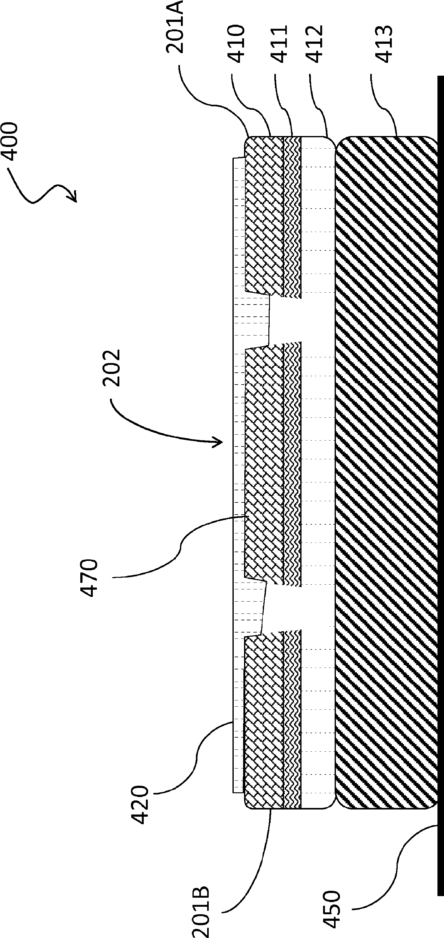
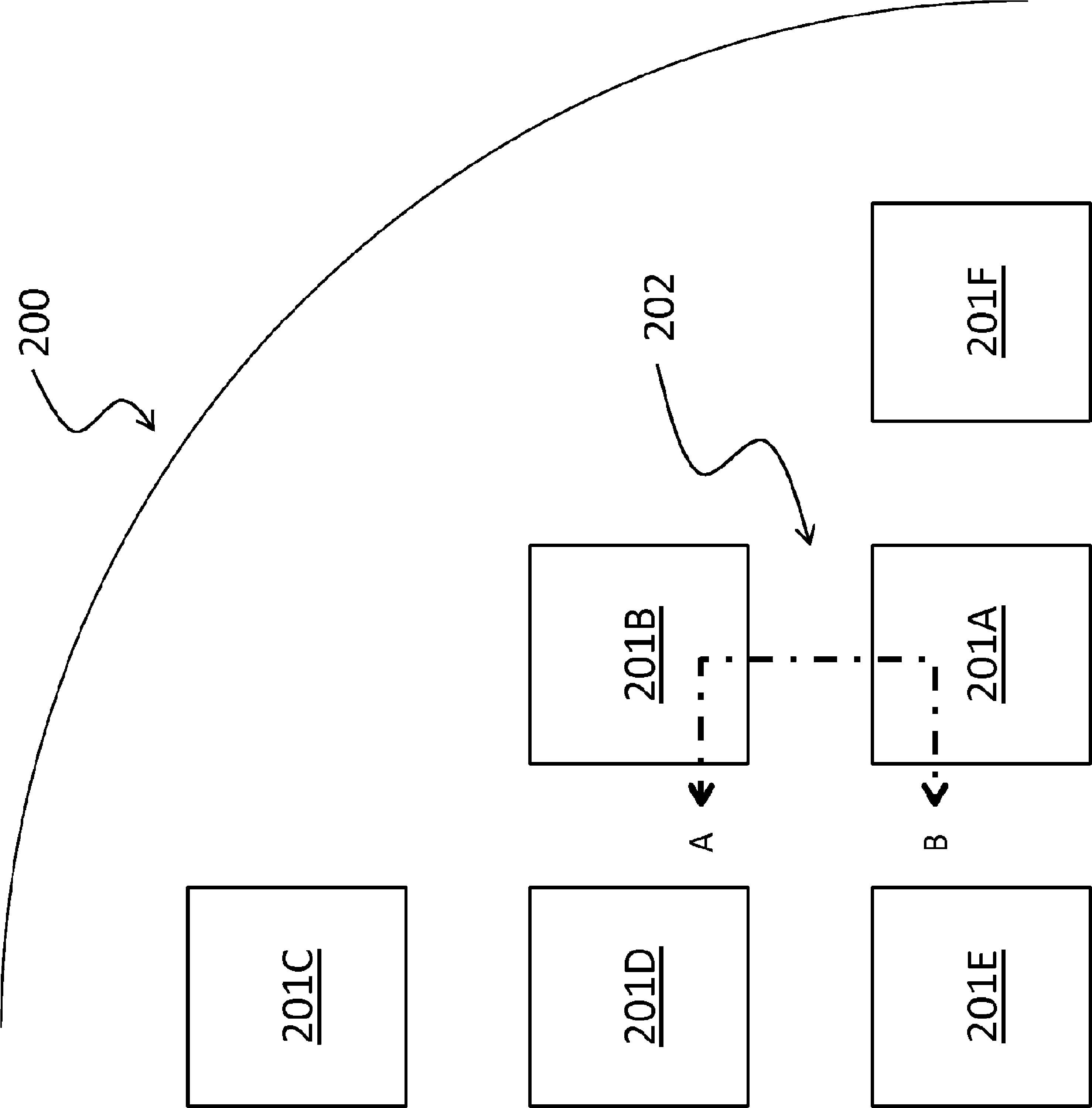
[0018] Although any type of semiconductor wafer divided into dies can utilize the present invention, in order to simplify the description, the remainder of the description will use wafers of square LED dies. Although the rest of this specification only mentions LEDs, the devices can be lasers, solar cells, detectors, DRAM, SRAM, ROM, flash memory, MEMS devices, microprocessors, logic gates, FPGAs, or any other suitable devices. Likewise, although a square die shape is described, any suitable die shape (or shapes) is contemplated and included within the scope of the present invention.
[0019] Although a substrate with an epitaxial layer is shown, other semiconductor configurations using non-epitaxial layers (for example, amorphous layers) are contemplated and included within the scope of the present invention. Although a wafer having an epitaxial layer and a substrate is shown, other configurations of wafers such as devices mounted to or bonded to a submount wafer are contemplate...
PUM
 Abstract
Description
Claims
Application Information
 - R&D
- Intellectual Property
- Life Sciences
- Materials
- Tech Scout
- Unparalleled Data Quality
- Higher Quality Content
- 60% Fewer Hallucinations
Browse by: Latest US Patents, China's latest patents, Technical Efficacy Thesaurus, Application Domain, Technology Topic, Popular Technical Reports.
© 2025 PatSnap. All rights reserved.Legal|Privacy policy|Modern Slavery Act Transparency Statement|Sitemap|About US| Contact US: help@patsnap.com