Touch screen and production thereof and touch display device
A touch screen and manufacturing method technology, applied in printed circuit manufacturing, printed circuit dielectrics, transparent dielectrics, etc., can solve the problems of whitening of metal connecting lines, breakdown of bridges, affecting touch functions, etc.
- Summary
- Abstract
- Description
- Claims
- Application Information
AI Technical Summary
Problems solved by technology
Method used
Image
Examples
Embodiment 1
[0041] An embodiment of the present invention provides a touch screen, such as figure 1 As shown, it includes: a transparent substrate 100, a patterned first transparent conductive layer 400 sequentially formed on the transparent substrate 100, a patterned insulating layer 500 and a patterned second transparent conductive layer 600; wherein, the first transparent conductive layer Among the layer 400 and the second transparent conductive layer 600 , one of them is formed with a plurality of driving lines, and the other is formed with a plurality of sensing lines; the pattern of the insulating layer 500 is consistent with the pattern of the second transparent conductive layer 600 .
[0042] In this embodiment, the patterned first transparent conductive layer 400 and the patterned second transparent conductive layer 600 are respectively provided through the insulating layer 500. If one of the two layers (400 and 600) forms a driving line, the other The specific patterns and desig...
Embodiment 2
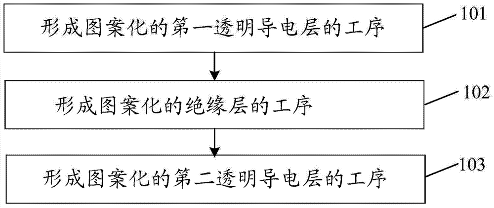
[0062] On the other hand, the embodiment of the present invention also provides a method for manufacturing a touch screen, such as image 3 As shown, the method includes:
[0063] 101. The process of forming a patterned first transparent conductive layer;
[0064] 102. A process of forming a patterned insulating layer;
[0065] 103. A process of forming a patterned second transparent conductive layer;
[0066] Among them, refer to figure 1 and figure 2 As shown, in the process 101 of forming the patterned first transparent conductive layer 400 and the process 103 of forming the patterned second transparent conductive layer 600, one process forms a plurality of driving lines, and the other process forms a plurality of sensing lines; The pattern of the insulating layer 500 formed in step 102 is consistent with the pattern of the first transparent conductive layer 400 , or consistent with the pattern of the second transparent conductive layer 600 .
[0067] The touch screen...
PUM
 Abstract
Description
Claims
Application Information


