
Voltage compensation oscillator circuit

A technology of voltage compensation and oscillator, which is applied in the field of voltage compensation oscillator circuit, can solve the problems of faster oscillation frequency, affecting the accuracy of oscillation frequency, and the oscillation frequency is easily affected by the power supply voltage, so as to reduce the increase range and improve The effect of precision

Active Publication Date: 2015-01-07
PUYA SEMICON SHANGHAI CO LTD
View PDF2 Cites 0 Cited by
  • Summary
  • Abstract
  • Description
  • Claims
  • Application Information

AI Technical Summary

Problems solved by technology

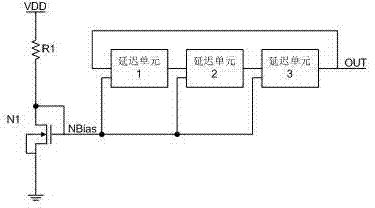
But the disadvantage of this circuit is that the oscillation frequency is easily affected by the power supply voltage. When the power supply voltage VDD becomes higher, the bias voltage NBias will also become higher, so that the delay unit becomes smaller and the oscillation frequency becomes faster, which affects the oscillation frequency. precision

Method used


Image

  • Voltage compensation oscillator circuit
  • Voltage compensation oscillator circuit
  • Voltage compensation oscillator circuit

Examples


Embodiment Construction

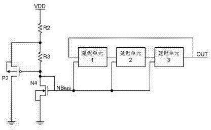
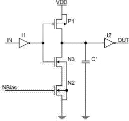
[0011] See figure 2 , image 3 As shown, a voltage compensation oscillator circuit includes a resistor R2, one end of the resistor R2 is connected to the power supply VDD, the other end of the resistor R2 is connected to the source end of the PMOS transistor P2, one end of the resistor R3, the other end of the resistor R3 and the gate end of the PMOS transistor P2 After being connected, connect the drain end of NMOS transistor N4, connect the gate end and drain end of NMOS transistor N4, and then connect multiple delay units, and multiple delay units are connected to form a ring, and the drain end of PMOS transistor P2 and the source end of NMOS transistor N4 are respectively Grounding; the delay unit includes three, respectively the first delay unit, the second delay unit, and the third delay unit, the output of the first delay unit is connected to the input of the second delay unit, and the output of the second delay unit is connected to the second delay unit The input end...


PUM


Abstract

The invention relates to the technical field of analogue integrated circuits, in particular to a voltage compensation oscillator circuit. The oscillation frequency of the voltage compensation oscillator circuit is hardly influenced by voltages of a power supply, and therefore the precision of the oscillation frequency is improved. The voltage compensation oscillator circuit comprises an NMOS transistor N4, a resistor R3 and multiple delay units. One end of the resistor R3 is connected with the drain end of the NMOS transistor N4, and the NMOS transistor N4 is connected with the multiple delay units after the drain end and the grate end of the NMOS transistor N4 are connected. The multiple delay units are connected to form a ring. The source end of the NMOS transistor N4 is grounded. The voltage compensation oscillator circuit is characterized by further comprising a resistor R2 and a PMOS transistor P2, wherein one end of the resistor R2 is connected with a power supply VDD, the other end of the resistor R2 is connected with the other end of the resistor R3 and the source end of the PMOS transistor P2, the grate end of the PMOS transistor P2 is connected with the drain end of the NMOS transistor N4, and the drain end of the PMOS transistor P2 is connected with the ground.

Description

technical field [0001] The invention relates to the technical field of analog integrated circuits, in particular to a voltage compensation oscillator circuit. Background technique [0002] Oscillator circuits are commonly used in the design of analog integrated circuits. An oscillator circuit involves such as figure 1 As shown, the resistor R1 and the N-type MOS transistor N1 form a bias voltage generating circuit, and the bias voltage NBias is generated at the gate terminal and the drain terminal connection of the NMOS transistor, and the bias voltage NBias is connected to several delay units, and these delay units Connect into a ring and keep oscillating. The number of delay units can be selected according to design requirements, so as to ensure that the loop formed by the delay units can oscillate and the oscillation frequency meets the requirements. The NBias voltage can control the delay time of the delay unit, thereby controlling the oscillation frequency of the enti...

Claims


Application Information

Patent Timeline
Patent Type & Authority Applications(China)
IPC IPC(8): H03B5/04
Inventor 童红亮陈涛李兆桂
Owner PUYA SEMICON SHANGHAI CO LTD
Learn More