Mixing-method-based method and system applied to defect detection of printed circuit board

A printed circuit board and defect detection technology, which is applied in the direction of optical testing for defects/defects, can solve problems such as poor fault tolerance, less connected domain segmentation and block detection methods, insufficient detection of image details, etc., and achieve good discrimination ability Effect

Active Publication Date: 2015-01-21
SOUTH CHINA UNIV OF TECH
View PDF7 Cites 28 Cited by
  • Summary
  • Abstract
  • Description
  • Claims
  • Application Information

AI Technical Summary

Problems solved by technology

Among them, the reference method has too strong dependence on the template, and adopts a matching algorithm similar to a simple error, which has poor fault tolerance for printed circuit board image deviation; the non-reference method relies more on rules than The disadvantages of matching specific image pixels are insufficient utilization of template information and insufficient detection of image details; the hybrid rule combines the advantages of the above two methods, and this method uses rules similar to the non-reference method Matching, at the same time, use the information on the template as much as possible, and further detect the detail pixels under the guidance of the rules
The hybrid method is still in its infancy, and there are few methods for connected domain segmentation and block detection

Method used


Image

  • Mixing-method-based method and system applied to defect detection of printed circuit board
  • Mixing-method-based method and system applied to defect detection of printed circuit board

Examples


Embodiment 1

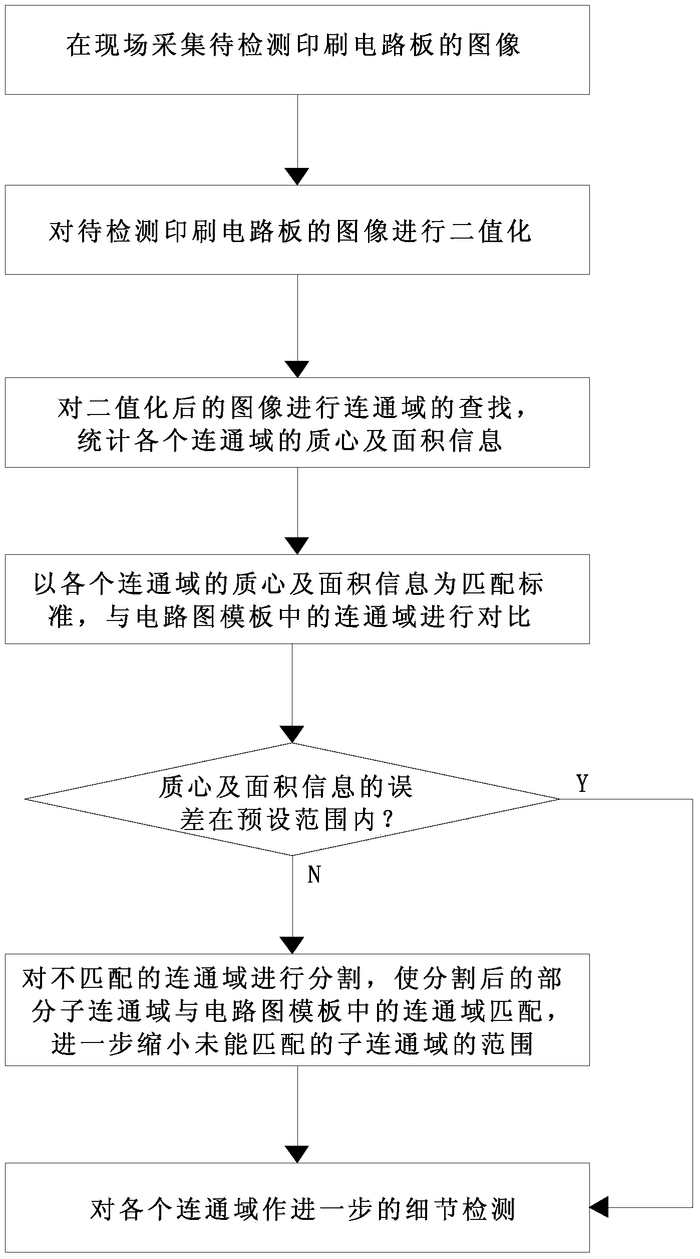
[0045] Such as figure 1 As shown, the printed circuit board defect detection method based on the hybrid method of the present embodiment includes the following steps:

[0046] 1) Collect images of printed circuit boards to be detected on site;

[0047] 2) binarize the image of the printed circuit board to be detected;

[0048] 3) search the connected domains for the binarized image, and count the centroid and area information of each connected domain;

[0049] 4) Using the centroid and area information of each connected domain as the matching standard, compare it with the connected domain in the circuit diagram template, if the error of the centroid and area information is within the preset range (such as 6% to 8%), it is considered a match, Otherwise, it is considered a mismatch;

[0050] 5) Segment the unmatched connected domains, make the segmented sub-connected domains match the connected domains in the circuit diagram template, and further narrow the scope of the unmat...

Embodiment 2

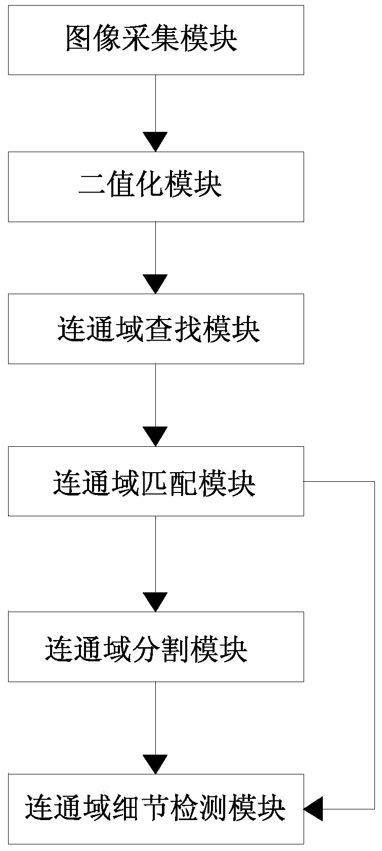
[0073] Such as figure 2 As shown, the printed circuit board defect detection system based on the hybrid method in this embodiment includes an image acquisition module, a binarization module, a connected domain search module, a connected domain matching module, a connected domain segmentation module, and a connected domain detail detection module, wherein:

[0074] The image acquisition module is used to collect images of printed circuit boards to be detected on site;

[0075] The binarization module is used to binarize the image of the printed circuit board to be detected;

[0076] The connected domain search module is used to search the connected domains of the binarized image, and count the centroid and area information of each connected domain;

[0077] The connected domain matching module is used to compare the centroid and area information of each connected domain with the connected domain in the circuit diagram template. If the error of the centroid and area informatio...


PUM


Abstract

The invention discloses a mixing-method-based method and a mixing-method-based system applied to defect detection of a printed circuit board. The method comprises the following steps: collecting an image of a to-be-detected printed circuit board in the field; carrying out binaryzation on the image of the to-be-detected printed circuit board; searching communication domains of the binaryzated image and counting information of mass center and area of each communication area; comparing each communication area with communication domains in a circuit diagram template by taking the information of mass center and area of each communication area as a matching standard, determining that the communication domains are matched with one another if the error of the information of mass center and area is in a predetermined range, or determining that the communication domains are unmatched with one another; cutting the unmatched communication domains, enabling part of secondary communication domains after cutting to be matched with the communication domains in the circuit diagram template, and further diminishing the range of the unmatched secondary communication domains; and further detecting each communication domain in detail. By virtue of the method and the system, the defect misinformation caused by rotating, horizontally moving, extending and retracting, inclining and the like can be well avoided; the reasonable deformation and defects can be well distinguished.

Description

technical field [0001] The invention relates to a defect detection method of a printed circuit board, in particular to a method and system for detecting a defect of a printed circuit board based on a hybrid method. The invention belongs to the technical field of defect detection. Background technique [0002] At present, there are three main methods of PCB defect detection: reference method, non-reference method and hybrid method. Among them, the reference method has too strong dependence on the template, and adopts a matching algorithm similar to a simple error, which has poor fault tolerance for printed circuit board image deviation; the non-reference method relies more on rules than The disadvantages of matching specific image pixels are insufficient utilization of template information and insufficient detection of image details; the hybrid rule combines the advantages of the above two methods, and this method uses rules similar to the non-reference method Matching, at ...

Claims


Application Information

Patent Timeline
Patent Type & Authority Applications(China)
IPC IPC(8): G01N21/88
Inventor 陈安陈暑生胡跃明
Owner SOUTH CHINA UNIV OF TECH
Why Eureka
Try Eureka