
Array substrate used in ADS (adaptive damping system) display device

A technology for array substrates and display devices, applied in nonlinear optics, instruments, optics, etc., can solve the problems of increased signal delay time, large resistance, and affecting the picture quality of display devices, etc.

Inactive Publication Date: 2015-01-21
BOE TECH GRP CO LTD +1
View PDF9 Cites 5 Cited by
  • Summary
  • Abstract
  • Description
  • Claims
  • Application Information

AI Technical Summary

Problems solved by technology

[0005] The present invention provides an array substrate applied to an ADS display device, which solves the problem in the prior art that the resistance of the entire common electrode network of the array substrate is very large, resulting in increased signal delay time and affecting the picture quality of the display device

Method used


Image

  • Array substrate used in ADS (adaptive damping system) display device
  • Array substrate used in ADS (adaptive damping system) display device
  • Array substrate used in ADS (adaptive damping system) display device

Examples


Embodiment Construction

[0018] An array substrate applied to an ADS display device according to an embodiment of the present invention will be described in detail below with reference to the accompanying drawings.

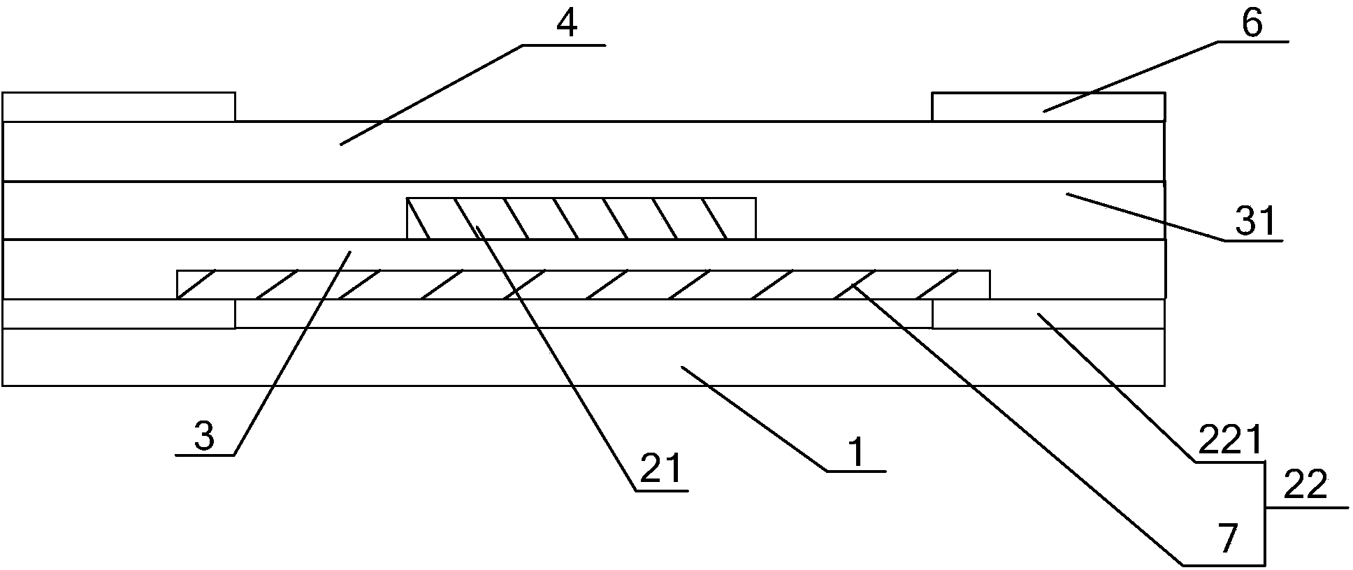
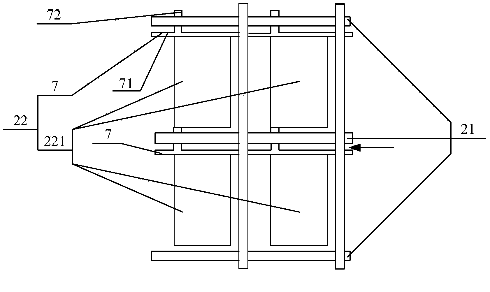
[0019] An embodiment of the present invention provides an array substrate applied to an ADS display device, such as figure 2 As shown, including a substrate 1, a common electrode layer 22 is arranged on the substrate 1, and a first insulating layer 3 is laid on the common electrode layer 22; a gate 21 is laid on the first insulating layer 3; Two insulating layers 31; a passivation layer 4 is laid on the second insulating layer 31, and a pixel electrode 6 is formed on the passivation layer 4; the common electrode layer 22 includes a common electrode 221 that is arranged on the substrate 1 at intervals, and is connected to adjacent The metal conductive layer 7 between the common electrodes 221; the metal conductive layer 7 is disposed corresponding to the non-display area.

[0020] An arr...


PUM


Abstract

The invention discloses an array substrate used in an ADS (adaptive damping system) display device, and relates to the technical field of display devices. The problems that the electrical resistance of a whole common electrode network of an array substrate in the prior art is quite high, so that signal delay time is prolonged, and the quality of images of the display device is high are solved. The array substrate used in the ADS display device comprises a substrate body, wherein a common electrode layer is arranged on the substrate body; a first insulating layer is paved on the common electrode layer; a grid electrode is arranged on the first insulating layer; a second insulating layer is paved on the grid electrode; a passivation layer is paved on the second insulating layer; a pixel electrode is formed on the passivation layer; the common electrode layer comprises common electrodes and metal conductive layers; the common electrodes are arranged on the substrate body at intervals; each metal conductive layer is connected between the two corresponding adjacent common electrodes; and the metal conductive layers correspond to a non-displaying region. The array substrate is mainly used in production of ADS display devices.

Description

technical field [0001] The present invention relates to the technical field of display devices, in particular to an array substrate applied in an ADS display device. Background technique [0002] Currently, liquid crystal displays have become mainstream products in display devices due to their advantages such as high responsiveness, high brightness, and high contrast. [0003] Among them, the liquid crystal display is mainly composed of an array substrate and a color filter substrate, and liquid crystal between the package and the two substrates; specifically, the working principle of the liquid crystal display is to control the rotation direction of the liquid crystal molecules through the action of the electric field on the liquid crystal, thereby achieve the purpose of display. In the prior art, the array substrate in ADS (edge ​​field effect type) display mode, such as figure 1 As shown, a glass substrate 1 is included, and a first electrode layer 2, an insulating laye...

Claims


Application Information

Patent Timeline
IPC IPC(8): G02F1/1343G02F1/1333
CPCG02F1/134309G02F1/1345G02F1/133397
Inventor 高玉杰
Owner BOE TECH GRP CO LTD
Learn More