Film forming method for metal blocking layer

A technology of metal barrier layer and film forming method, which is applied in the direction of electrical components, semiconductor/solid-state device manufacturing, circuits, etc., can solve the problem of filling barrier layer voids, etc., to reduce barrier layer and substrate voids, simple and efficient process, prevent damage effect

Inactive Publication Date: 2015-01-21
SHANGHAI HUAHONG GRACE SEMICON MFG CORP
View PDF3 Cites 5 Cited by
  • Summary
  • Abstract
  • Description
  • Claims
  • Application Information

AI Technical Summary

Problems solved by technology

[0004] The technical problem to be solved by the present invention is to provide a method for forming a metal barrier layer, which can solve the problem of voids in the existing through-hole filling barrier layer, and effectively improve product yield

Method used


Image

  • Film forming method for metal blocking layer
  • Film forming method for metal blocking layer
  • Film forming method for metal blocking layer

Examples


Embodiment Construction

[0029] The film forming method of the metal barrier layer of the present invention, the flowchart is as figure 2 As shown, the specific steps include:

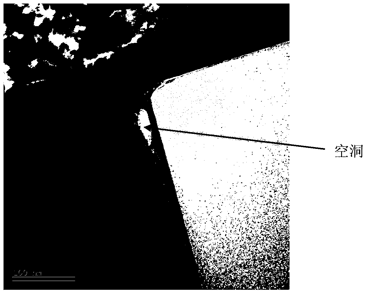
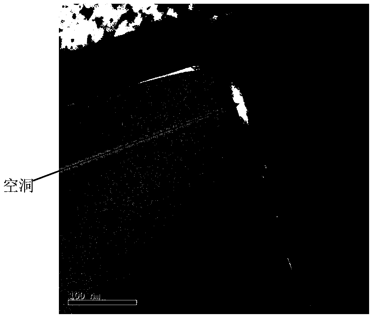
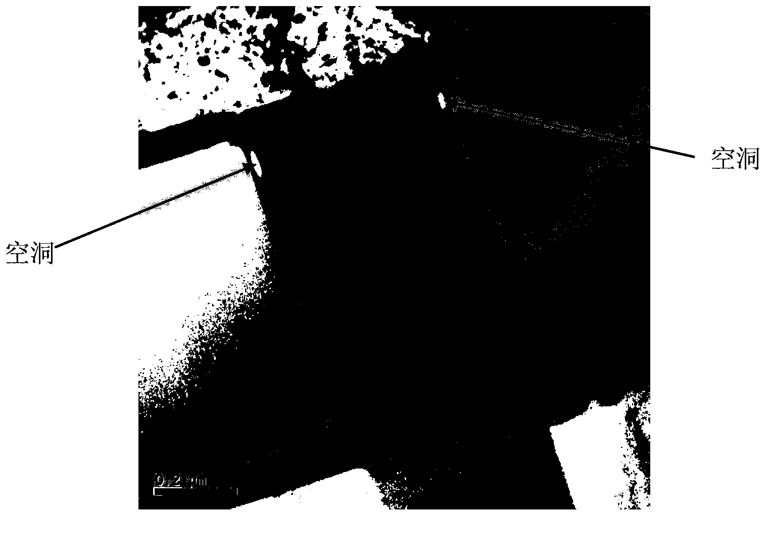
[0030] 1) On the silicon wafer (such as the oxide layer 2 of the substrate silicon 1), dry etching is used to etch the through hole 3 (such as image 3 Shown);

[0031] 2) A first barrier metal layer is formed on the sidewall and bottom of the via 3, where the first barrier metal layer is composed of the Ti layer 4 as the bottom layer and the first TiN layer 5 on the Ti layer 4 (such as Figure 4-5 Shown);

[0032] In addition, the method of forming the first metal barrier layer in this step may be as follows:

[0033] After the Ti layer 4 is formed by a metal physical sputtering method, the first TiN layer 5 is formed by a metal chemical vapor deposition method; wherein the sputtering temperature is 100 to 500° C., and the sputtering pressure is 1 to 10 torr; The deposition temperature is 200~600℃, and the deposition pressure is 1~1...


PUM

PropertyMeasurementUnit
thicknessaaaaaaaaaa
thicknessaaaaaaaaaa

Abstract

The invention discloses a film forming method for a metal blocking layer. The method comprises steps that: 1), through hole etching on a silicon sheet is carried out; 2), a first metal blocking layer is formed on a side wall and a bottom portion of a through hole, and the first metal blocking layer comprises a Ti layer as the bottom layer and a first TiN layer on the Ti layer; 3) a second metal blocking layer is formed on the surface of the first TiN layer, the second metal blocking layer is the second TiN layer, and oxygen content of the second TiN layer is lower than that of the first TiN layer; and 4), annealing processing is carried out. The method can solve a problem of cavity generation in a through hole filling blocking layer and can effectively improve the product yield.

Description

Technical field [0001] The present invention relates to a method for forming a film in a semiconductor integrated circuit, in particular to a method for forming a metal barrier layer. Background technique [0002] With the development of semiconductor devices to the deep sub-micron size, the density and complexity of the devices continue to increase, and the requirements for the process are becoming more and more demanding. As a channel for interconnection of multilayer metal layers and connections between devices and external circuits, through holes play a very important role in device configuration. [0003] In the existing through-hole manufacturing method, the size of the through-hole is getting smaller and smaller, and when the through-hole is formed, the adhesion of the barrier layer to the substrate becomes poor, the stress of the barrier layer changes greatly, and it is easy to produce Hole, as shown in Figure 1. The generation of voids will lead to high through-hole resi...

Claims


Application Information

Patent Timeline
Patent Type & Authority Applications(China)
IPC IPC(8): H01L21/768
CPCH01L21/76877H01L23/53295
Inventor 刘善善费强李晓远
Owner SHANGHAI HUAHONG GRACE SEMICON MFG CORP
Why Eureka
Try Eureka