A multilayer printed circuit board

A multi-layer printing and circuit board technology, applied in the field of electronics, can solve the problems of copper skin blistering, board warping, thermal expansion and contraction, etc., to ensure the contact condition, ensure normal work, and relieve the effect of expansion

Active Publication Date: 2017-07-21
TCL CHINA STAR OPTOELECTRONICS TECH CO LTD
View PDF3 Cites 0 Cited by
  • Summary
  • Abstract
  • Description
  • Claims
  • Application Information

AI Technical Summary

Problems solved by technology

When the residual copper ratio of each layer of a multilayer printed circuit board is different, when the temperature is high, the thermal expansion and contraction of each layer are different due to the different residual copper ratio of each layer, and board bending may occur. , board warping, copper skin blistering and other bad problems
[0003] The inventor found that bad problems such as board bending, board warping, and copper blistering will affect the contact between the electronic components carried by the multilayer printed circuit board and the solder joints of the multilayer printed circuit board, and even lead to the multilayer printed circuit board. layer printed circuit board failure

Method used


Image

  • A multilayer printed circuit board
  • A multilayer printed circuit board
  • A multilayer printed circuit board

Examples


Embodiment Construction

[0025] The implementation of the present invention will be described in detail below in conjunction with the accompanying drawings and examples, so as to fully understand and implement the process of how to apply technical means to solve technical problems and achieve technical effects in the present invention. It should be noted that, as long as there is no conflict, each embodiment and each feature in each embodiment of the present invention can be combined with each other, and the formed technical solutions are all within the protection scope of the present invention.

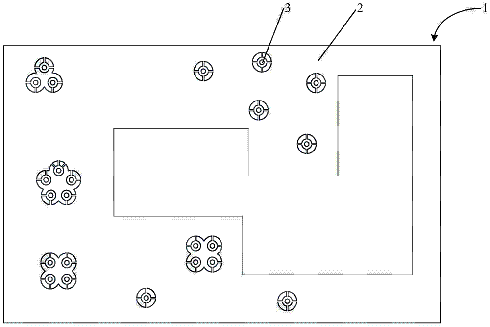
[0026] Embodiments of the present invention provide a multilayer printed circuit board, such as figure 1 As shown, the multilayer printed circuit board includes:

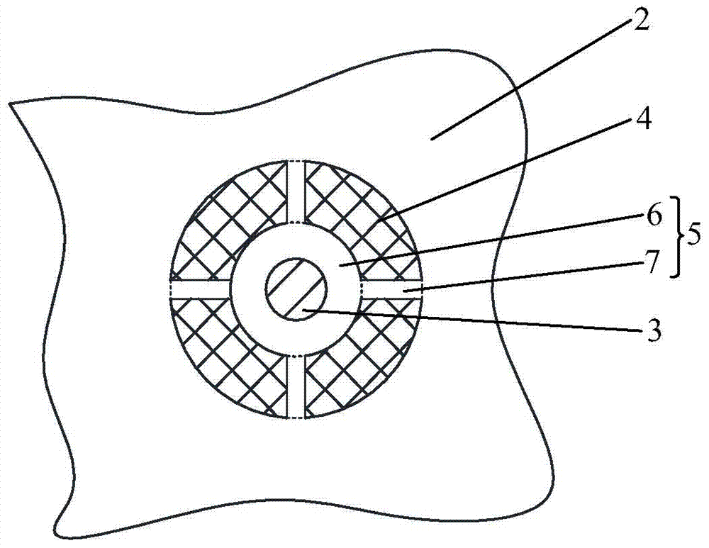
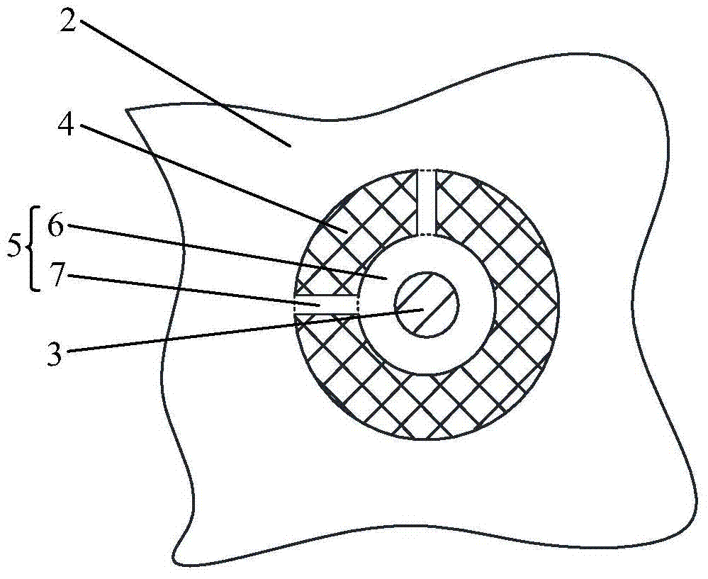
[0027] It includes a plurality of alternately stacked wiring layers 1 and isolation layers 4 , any wiring layer 1 includes a copper skin 2 , and the copper skin 2 of each layer of the same network is conducted through a via hole 3 .

[0028] In t...


PUM


Abstract

The present invention relates to the technical field of electronics. Disclosed is a multilayer printed circuit board, which can prevent the problems such as board bending, board warping and copper sheet blistering caused by different residual copper rates of various layers. The multilayer printed circuit board comprises multiple wiring layers and isolating layers that are superimposed alternately. Any wiring layer comprises a copper sheet, and the copper sheets in the same network on the layers are conducted through via holes.

Description

technical field [0001] The invention relates to the field of electronic technology, in particular to a multilayer printed circuit board. Background technique [0002] As we all know, a multilayer printed circuit board (Printed Circuit Board, PCB for short) is widely used in various products with high density of electronic components. Multilayer printed circuit boards are mostly formed by alternately stacking wiring layers and isolation layers. With the popularization of Surface Mount Technology (SMT for short), more stringent requirements are put forward for the bending and warping of multilayer printed circuit boards. When the residual copper ratio of each layer of a multilayer printed circuit board is different, when the temperature is high, the thermal expansion and contraction of each layer are different due to the different residual copper ratio of each layer, and board bending may occur. , board warping, copper skin blistering and other bad problems. [0003] The in...

Claims


Application Information

Patent Timeline
Patent Type & Authority Patents(China)
IPC IPC(8): H05K1/02
CPCH05K1/0271H05K1/0298H05K1/115H05K1/02
Inventor 符俭泳
Owner TCL CHINA STAR OPTOELECTRONICS TECH CO LTD
Why Eureka
Try Eureka