Manufacturing method and screen printing method of solder-masked and screen-printed nail bed and solder-masked and screen-printed nail bed

A production method and screen printing technology, which is applied to screen printing machines, printing machines, printing machines, etc., can solve problems such as damage to PCB boards, long time-consuming cloth nails, and dislocation of cloth nails, so as to avoid wrong nailing positions and stabilize positioning High performance and improved stability

Active Publication Date: 2015-02-18
GUANGZHOU FASTPRINT CIRCUIT TECH +2
View PDF6 Cites 13 Cited by
  • Summary
  • Abstract
  • Description
  • Claims
  • Application Information

AI Technical Summary

Problems solved by technology

[0007] The above-mentioned process is cumbersome in practical application. Bed nails need to be placed in different positions for panels with different graphics during production. This requires operators to have rich experience in nailing, otherwise it will take a long time to set nails and prone to nails Misalignment, causing damage to the PCB board during silk screen printing

Method used


Image

  • Manufacturing method and screen printing method of solder-masked and screen-printed nail bed and solder-masked and screen-printed nail bed
  • Manufacturing method and screen printing method of solder-masked and screen-printed nail bed and solder-masked and screen-printed nail bed
  • Manufacturing method and screen printing method of solder-masked and screen-printed nail bed and solder-masked and screen-printed nail bed

Examples


Embodiment Construction

[0035] In order to facilitate the understanding of the present invention, the present invention will be described more fully below with reference to the associated drawings. Preferred embodiments of the invention are shown in the accompanying drawings. However, the present invention can be embodied in many different forms and is not limited to the embodiments described herein. On the contrary, these embodiments are provided to make the understanding of the disclosure of the present invention more thorough and comprehensive.

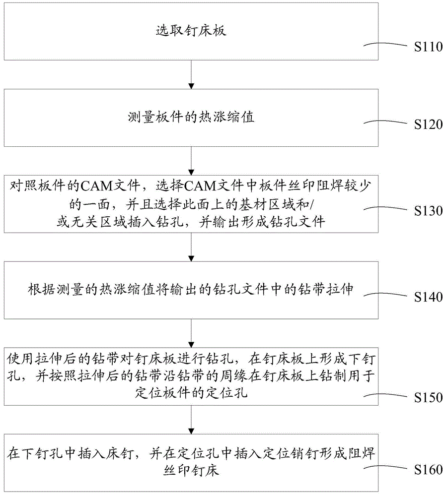
[0036] Such as figure 1 As shown, the manufacturing method of the solder resist silk screen nail bed in one embodiment includes the following steps:

[0037] Step S110: Select the bed of nails board.

[0038] The size of the bed of nails board should be slightly larger than the size of the board to be screen-printed and soldered, that is, the size of the bed of nails should be such that when the board to be screen-printed and soldered is placed on the ...


PUM


Abstract

The invention relates to a manufacturing method and screen printing method of a solder-masked and screen-printed nail bed and the solder-masked and screen-printed nail bed. Nail distributing efficiency and nail distributing accuracy can be improved. According to the manufacturing method of the solder-masked and screen-printed nail bed, the nail distribution positions of the nail bed are obtained through CAM file manufacturing, a drill band is stretched and adjusted according to the heat expansion and contraction value of a plate to be screen-printed and solder-masked, and therefore the precision of the nail distribution positions is high. Through the method, operators can be prevented from mechanically looking for the nail distribution positions, efficiency is high, the situation that the nailing positions are wrong due to the fact that the experience of staff is insufficient can be avoided, and high operability is achieved.

Description

technical field [0001] The invention relates to the field of circuit board production, in particular to a method for manufacturing a solder resist silk screen nail bed, a silk screen printing method and a solder resist silk screen nail bed. Background technique [0002] With the development of the electronics industry towards high density, thinness, miniaturization, and high reliability, the requirements for wiring density of circuit boards are getting higher and higher. The gradual increase of circuit board wiring density requires the spacing of SMT solder pins to be smaller and smaller, which reduces the width of the solder resist bridge that prevents solder bridging, resulting in the increasingly prominent problem of solder resist bridge drop. Nowadays, silk screen printing is commonly used to make solder mask bridges, such as ordinary silk screen printing and bed of nails screen printing. Among them, the use of bed of nails screen printing can achieve the same pre-bakin...

Claims


Application Information

Patent Timeline
Patent Type & Authority Applications(China)
IPC IPC(8): H05K3/28B41F15/18
CPCH05K3/28H05K2203/15
Inventor 袁处钱进金宇星
Owner GUANGZHOU FASTPRINT CIRCUIT TECH
Why Eureka
Try Eureka