A liquid crystal display device and manufacturing method thereof

A technology of a liquid crystal display device and a manufacturing method, which is applied in the fields of nonlinear optics, instruments, optics, etc., and can solve problems such as abnormal gaps between array substrates, color filter substrates, squeezed light leakage, crushed bright spots, etc., to achieve enhanced standing stability, Improve the effect of light leakage or crushed bright spots

Active Publication Date: 2017-11-10
XIAMEN TIANMA MICRO ELECTRONICS +1
View PDF6 Cites 0 Cited by
  • Summary
  • Abstract
  • Description
  • Claims
  • Application Information

AI Technical Summary

Problems solved by technology

[0004] When the array substrate and the color filter substrate are aligned and bonded, due to the flatness of the standing position of the columnar spacer, the Main PS or Sub PS may slide into the through hole for electrically connecting the pixel electrode and the drain, resulting in Squeeze light leakage or crushed bright spots, and the gap between the array substrate and the color filter substrate is abnormal after the Main PS or Sub PS slips

Method used


Image

  • A liquid crystal display device and manufacturing method thereof
  • A liquid crystal display device and manufacturing method thereof
  • A liquid crystal display device and manufacturing method thereof

Examples


Embodiment Construction

[0025] The present invention will be further described in detail below in conjunction with the accompanying drawings and embodiments. It should be understood that the specific embodiments described here are only used to explain the present invention, but not to limit the present invention. In addition, it should be noted that, for the convenience of description, only parts related to the present invention are shown in the drawings but not all of them, and the same or similar symbols in the drawings represent the same or similar elements or have the same or similar functions components.

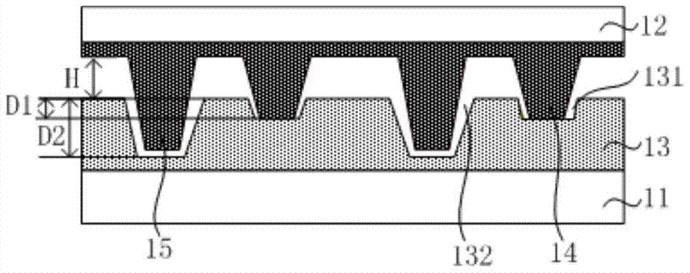
[0026] See figure 1 , figure 1 It is a cross-sectional view of a liquid crystal display device provided by an embodiment of the present invention. The liquid crystal display device includes a first substrate 11, a second substrate 12 opposite to the first substrate 11, and a first flat surface on the first substrate 11. The first planarization layer 13 is provided with a first deep hole 131...


PUM


Abstract

The invention discloses a liquid crystal display device and a manufacturing method of the liquid crystal display device. The liquid crystal display device comprises a first substrate, a second substrate, a first planarization layer, first photo spacers and second photo spacers, wherein the first substrate and the second substrate are arranged oppositely; the first planarization layer is located on the first substrate and provided with first deep holes and second deep holes; the first ends of the first photo spacers are arranged on the second substrate, and the second ends of the first photo spacers are arranged in the first deep holes and make contact with the bottoms of the first deep holes; the first ends of the second photo spacers are arranged on the second substrate, the second ends of the second photo spacers are arranged in the second deep holes, and gaps are reserved between the second ends of the second photo spacers and the bottoms of the second deep holes. By the adoption of the liquid crystal display device, the standing stability of the photo spacers can be enhanced, the phenomenon that light leaks or bright spots are broken due to sliding of the photo spacers can be relieved, the number of mask plates used in the process of preparing the liquid crystal display device can be reduced, the preparation process is simplified, and the preparation cost is lowered.

Description

technical field [0001] The invention relates to the technical field of liquid crystal display, in particular to a liquid crystal display device and a manufacturing method thereof. Background technique [0002] Thin Film Transistor Liquid Crystal Display (TFT-LCD) has become a display technology that can span all sizes due to its small size, low power consumption, and no radiation. It is widely used in fields such as TVs and notebooks. computer, monitor or mobile phone etc. [0003] TFT-LCD is a liquid crystal cell formed by aligning and bonding the array substrate and the color filter substrate. A columnar spacer (Photot Spacer, PS) is used to maintain the cell thickness of the liquid crystal cell. At present, the main design method adopted for the PS in TFT-LCD is to apply the main PS (Main PS) and the auxiliary PS (Sub PS) to play a supporting role together, wherein there is a certain height difference between the Main PS and the Sub PS, and The number of Main PS is sma...

Claims


Application Information

Patent Timeline
Patent Type & Authority Patents(China)
IPC IPC(8): G02F1/1339G02F1/1333
CPCG02F1/1333G02F1/13394
Inventor 张磊周秀峰
Owner XIAMEN TIANMA MICRO ELECTRONICS
Why Eureka
Try Eureka