
Eureka
For R&D, Eureka makes reading and utilizing patents & technical documents easy.
Eureka AIR
Designed for self-driven R&D workflows. Generate viable solutions, solve complex R&D challenges, empower your innovation with AI.

Eureka Materials
Designed for material experts only. Revolutionize your material R&D, from search, analyze, to developing new materials.

TechResearch
Generate reliable direction feasibility study reports for your R&D in just a few steps.

TechSeek
Discover and master advanced knowledge NOW. Basics, ideas, possibilities, all at once.

TechMind
As an expert in R&D Theories, TechMind can generates customized viable solutions instantly.

TechRisk
Analyze your overall solution with one click, know your potential R&D risks in advance.

TechMonitor
Get weekly tech updates, stay abreast of the latest tech innovations and key insights.
Substrate, display panel and display device
A technology for display panels and substrates, applied in static indicators, optics, instruments, etc., to solve problems such as VSR circuit breakdown, burnout, and abnormal panel screen display.
- Summary
- Abstract
- Description
- Claims
- Application Information
AI Technical Summary
Problems solved by technology
Method used
Image

Examples
Embodiment 1
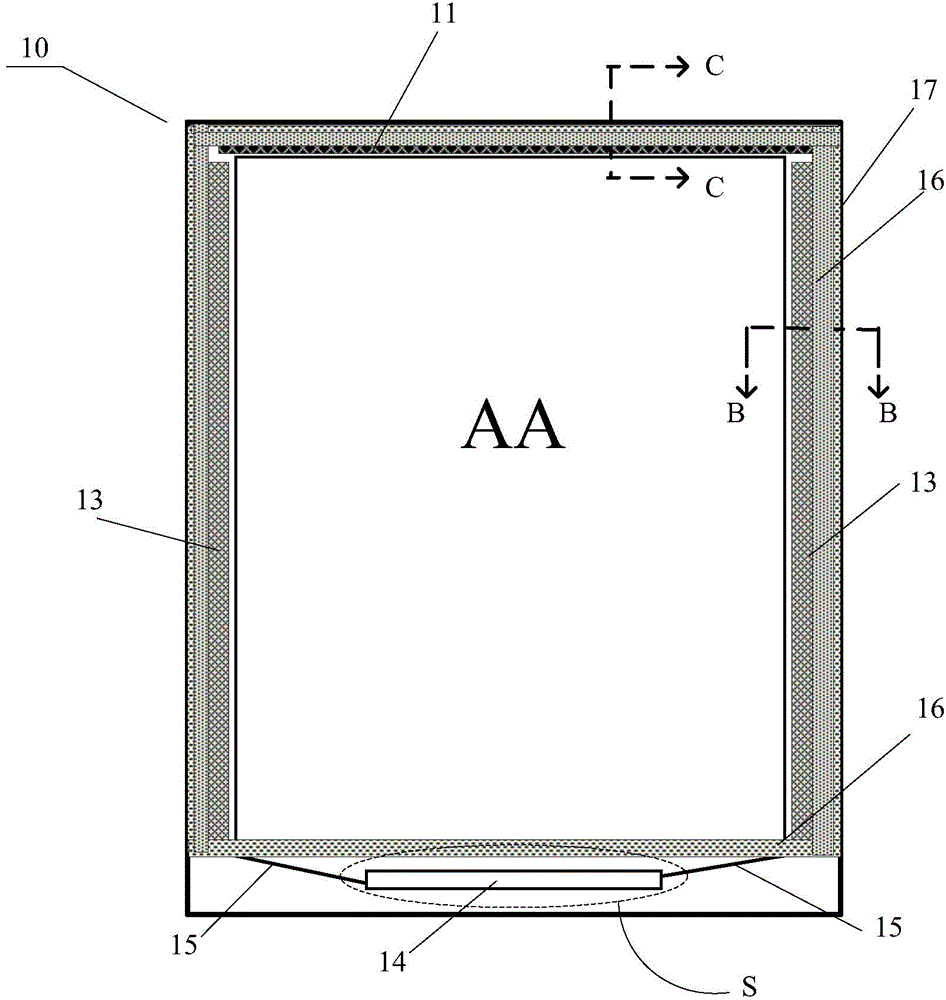
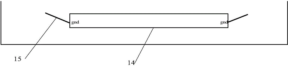
[0024] figure 1 Shown is a schematic view of the structure of the substrate provided by the preferred embodiment of the present invention, such as figure 1 As shown, the substrate 10 includes a base substrate (not shown in the figure), and the base substrate is divided into an AA area (display area), and a gate drive circuit 13, an electrostatic protection circuit 11 (ESD), and an electrostatic protection circuit 11 (ESD) are arranged on the periphery of the AA area. Drive unit 14. Generally, the gate driving circuit 13 is disposed on the left and right sides of the AA area, and the electrostatic protection circuit 11 is disposed on the upper side of the AA area and the upper and lower ends of the gate driving circuit 13 . However, the gate drive circuit of some substrates is installed on the side of the AA area, and the location of the electrostatic protection circuit is also different. figure 1 What is shown is only for illustration, and does not constitute a limitation to...
Embodiment 2
[0033] Figure 5 A schematic diagram of another substrate structure provided for a preferred embodiment of the present invention, such as Figure 5 As shown, the substrate 10 includes a base substrate (not shown in the figure), and the base substrate is divided into an AA area (display area), and a gate drive circuit 13, an electrostatic protection circuit 11 (ESD), and an electrostatic protection circuit 11 (ESD) are arranged on the periphery of the AA area. Drive unit 14. Generally, the gate driving circuit 13 is disposed on the left and right sides of the AA area, and the electrostatic protection circuit 11 is disposed on the upper side of the AA area and the upper and lower ends of the gate driving circuit 13 . However, the gate drive circuit of some substrates is arranged on the side of the AA area, and the location of the electrostatic protection circuit is also different. figure 1 What is shown is only for illustration, and does not constitute a limitation to the prot...
Embodiment 3
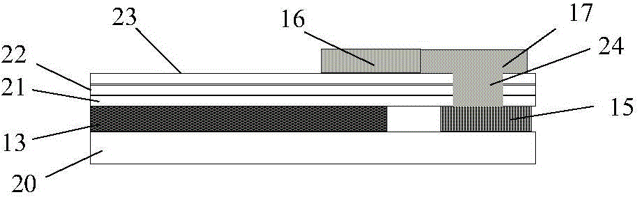
[0037] Image 6 A schematic structural diagram of a display panel provided for a preferred embodiment of the present invention, such as Image 6 As shown, the display panel includes a first substrate and a second substrate. The structure of the first substrate is the same as that provided in Embodiment 1 or Embodiment 2 above. A drive unit 14 and a signal interface area 18 are arranged on the first substrate. Notably, there may be more than one driving unit 14 on the display panel. If there is a gate driving unit and a data driving unit, the signal interface area 18 may also be more than one or may not exist according to the specific product design. Image 6 It is only for illustrating the present invention, and does not constitute a limitation to the protection scope of the present invention. The first substrate and the second substrate are hermetically bonded by a sealant (not shown in the figure). Since the first substrate is provided with a conductive frame glue and is e...
PUM
 Abstract
Description
Claims
Application Information
 - R&D Engineer
- R&D Manager
- IP Professional
- Industry Leading Data Capabilities
- Powerful AI technology
- Patent DNA Extraction
Browse by: Latest US Patents, China's latest patents, Technical Efficacy Thesaurus, Application Domain, Technology Topic, Popular Technical Reports.
© 2024 PatSnap. All rights reserved.Legal|Privacy policy|Modern Slavery Act Transparency Statement|Sitemap|About US| Contact US: help@patsnap.com