Test point arrangement method for integrated circuit board

A technology of integrated circuit board and layout method, applied in the direction of electronic circuit testing, etc., can solve the problems of unoptimized processing layout, low precision, irregularity, etc., to facilitate subsequent debugging, improve utilization, and facilitate wiring. Effect

Active Publication Date: 2015-03-11
湖州丰源农业装备制造有限公司
View PDF8 Cites 1 Cited by
  • Summary
  • Abstract
  • Description
  • Claims
  • Application Information

AI Technical Summary

Problems solved by technology

When making a fixture, it is necessary to locate each test point, which requires a lot of work and low precision. After the test points of the fixture reach a certain level, maintenance is very complicated due to too many leads. Distributed test points also reduce the debugging speed of developers
[0004] In the prior art, the test points are randomly distributed on the main board of the mobile terminal, and they are placed in a seam-like manner without optimizing the layout, which brings design and maintenance to the development personnel who need to use the test points for subsequent debugging and the production of production fixtures. If the test points are randomly distributed, it means that there must be corresponding test pins on the test fixture that can touch the test points. In this way, the coordinates of the test pins on the test fixture are also chaotic and irregular. It brings a huge workload and also brings huge complexity to the maintenance of the fixture

Method used


Image

  • Test point arrangement method for integrated circuit board
  • Test point arrangement method for integrated circuit board
  • Test point arrangement method for integrated circuit board

Examples


Embodiment Construction

[0053] The present invention will be further elaborated below by describing a preferred specific embodiment in detail in conjunction with the accompanying drawings.

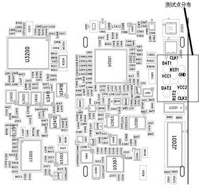
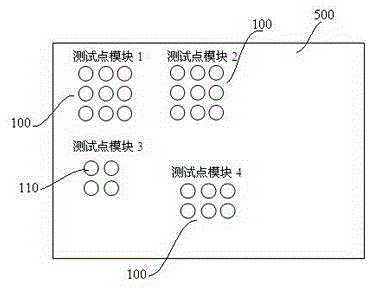
[0054] Such as Figure 2-Figure 6 As shown, a test module for integrated circuit board testing, the test module includes: a plurality of test point modules 100 , a plurality of test pin modules 200 and a plurality of test point combination modules 300 . Wherein, each test point module 100 is distributed and arranged on the integrated circuit board 500 , and the test point module 100 is composed of a plurality of test points 110 with the same function, and the plurality of test points 110 are arranged on the integrated circuit board 500 at equal intervals. Each test pin module 200 is connected to the corresponding test point module 100 for testing.

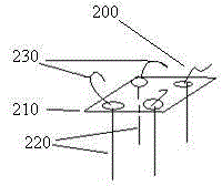
[0055] Such as figure 2 , Figure 4-Figure 6 As shown, in this embodiment, according to the actual situation of the integrated circuit board 500, the shape of the...


PUM


Abstract

The invention discloses a test point arrangement method for an integrated circuit board. The method comprises the following steps: according to the area size of the integrated circuit board and the number of test points having the same function, selecting test point module positions; according to the area size of the test point module positions and the number of the test points having the same function, arranging test point modules on the integrated circuit board; and according to the area size of the test point modules and the number of the test points, manufacturing test needle modules matching the test point modules. According to the test point arrangement method for the integrated circuit board, the test points on the integrated circuit board are arranged in a modularization mode according to functions; and it is agreed that the distances between each test point and corresponding adjacent test points are the same, the test point areas on the integrated circuit board look tidy and regular, and debugging personnel can conveniently find each test point with the functions within one function module.

Description

technical field [0001] The invention relates to a testing and debugging method for an integrated circuit board, in particular to a layout method for testing points of an integrated circuit board. Background technique [0002] In the prior art, the test points on the mobile terminal are mainly used to facilitate R&D personnel to test the internal signals of the mobile terminal. In production, the test points are also used to perform necessary tests on the main board functions. All test points are essential functional units of the mobile terminal. [0003] With more and more functions on the mobile terminal, the number of test points used for debugging and production is also increasing day by day, and the device area on the mobile terminal is also getting smaller and smaller, resulting in the distribution of test points everywhere. When making a fixture, it is necessary to locate each test point, which requires a lot of work and low precision. After the test points of the fixt...

Claims


Application Information

Patent Timeline
Patent Type & Authority Applications(China)
IPC IPC(8): G01R31/28
Inventor 杨大江
Owner 湖州丰源农业装备制造有限公司
Why Eureka
Try Eureka