Semiconductor device
A technology for semiconductors and devices, applied in the field of semiconductor devices, can solve the problems of small contact area between metal electrodes and GaN semiconductor devices, limited heat dissipation performance of GaN semiconductor devices, and poor air flow of packaging tubes, so as to improve the heat dissipation effect and reduce the temperature. , the effect of improving reliability
- Summary
- Abstract
- Description
- Claims
- Application Information
AI Technical Summary
Problems solved by technology
Method used
Image

Examples
Embodiment 1
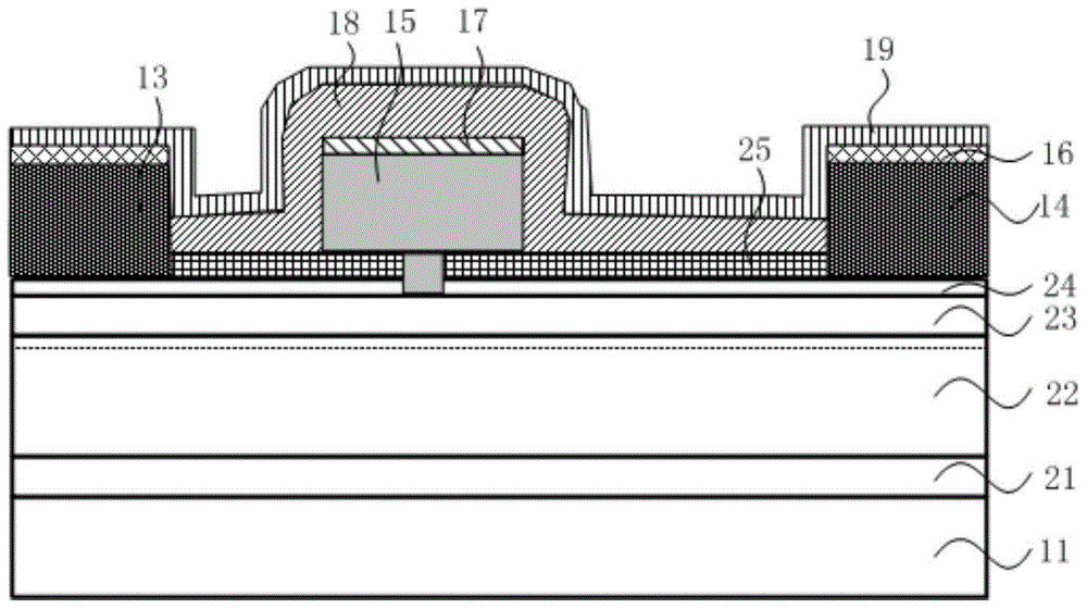
[0054] figure 1 A schematic cross-sectional structure diagram of a semiconductor device provided by Embodiment 1 of the present invention is shown, figure 2 It shows a schematic top view structure of the semiconductor device provided by Embodiment 1 of the present invention, combined with figure 1 and figure 2 Embodiment 1 of the present invention will be described.
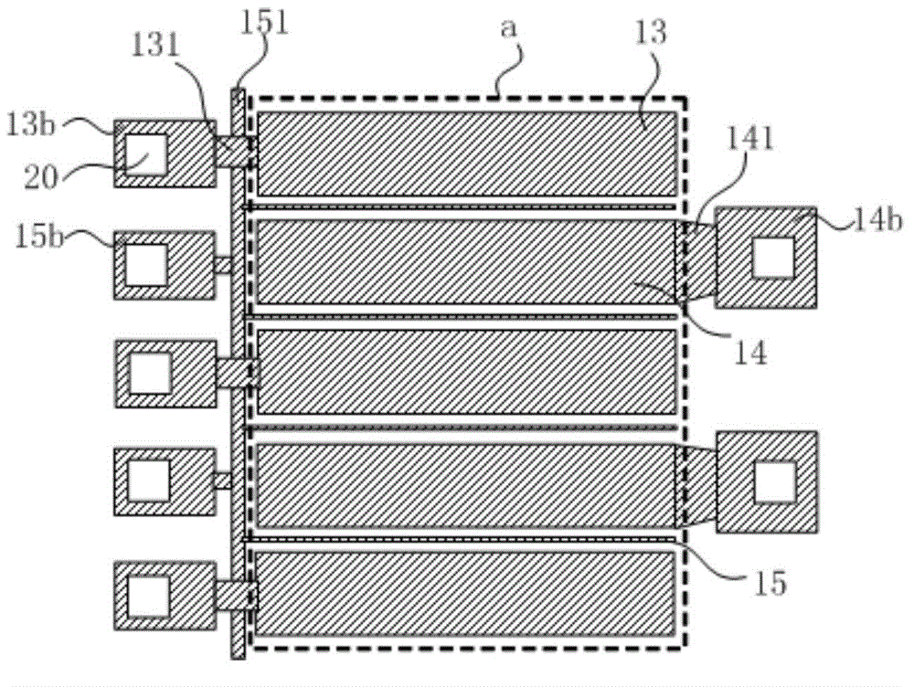
[0055] See figure 1 and figure 2 , the semiconductor device includes: a substrate 11, a multilayer semiconductor layer on the substrate 11, the multilayer semiconductor layer includes an active region a and an inactive region, and the region outside the active region a is the inactive region , a source electrode and a drain electrode located on the multi-layer semiconductor layer, the source electrode and the drain electrode include a source electrode 13 and a drain electrode 14 located in the active region a and a source electrode 13b located in the passive region and the drain electrode 14b, the gate lo...
Embodiment 2
[0079] image 3 shows a schematic top view of the semiconductor device provided by Embodiment 2 of the present invention, Figure 4 shows a schematic diagram of the cross-sectional temperature of a semiconductor device in the prior art, Figure 5 It shows the cross-sectional temperature schematic diagram of the semiconductor device provided by the second embodiment of the present invention, combined with Figure 3 to Figure 5 Embodiment 2 of the present invention will be described.
[0080] The semiconductor device provided in Embodiment 2 of the present invention is based on the semiconductor device provided in Embodiment 1 above, and the same parts as the semiconductor device in Embodiment 1 will not be described again.
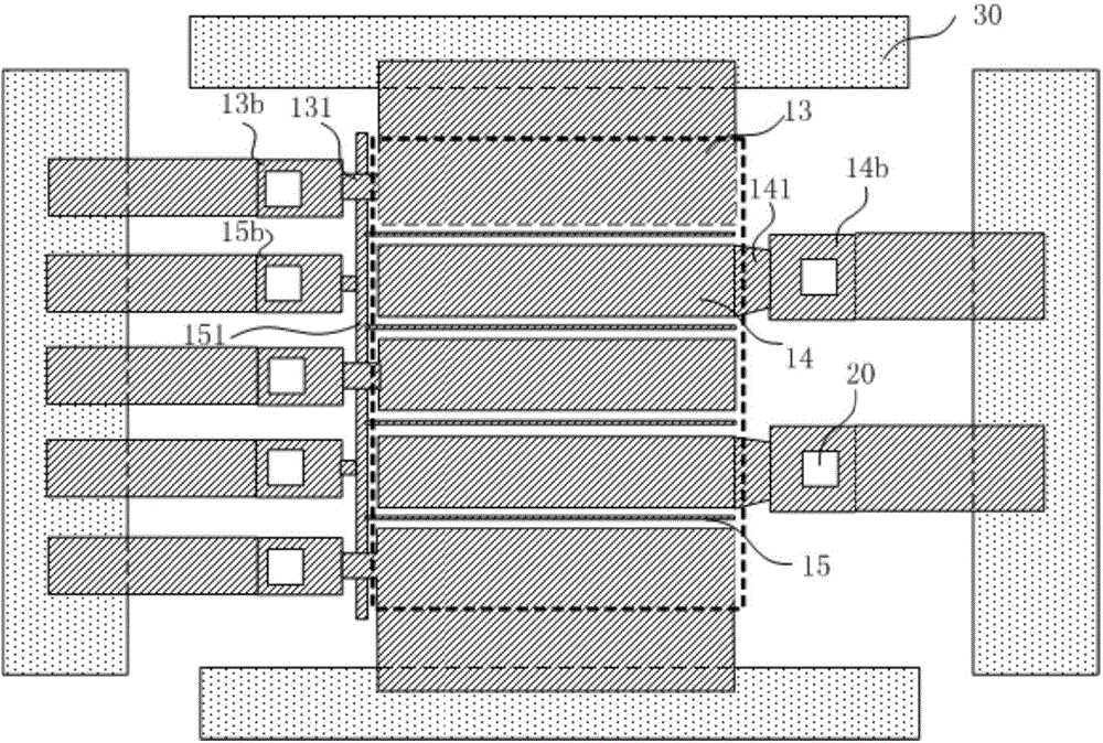
[0081] The semiconductor device provided by Embodiment 2 of the present invention further includes a heat sink 30 arranged around the edge of the passive area, and the second heat dissipation layer 16 is connected to the heat sink 30 .
[0082] In this e...
Embodiment 3
[0088] Figure 6 A schematic diagram showing the cross-sectional structure of the active region of the semiconductor device provided by Embodiment 3 of the present invention, please refer to Figure 6 , the semiconductor device includes: a substrate 11, a multilayer semiconductor layer positioned on the substrate 11, the multilayer semiconductor layer includes an active region a and a passive region ( Figure 6 not shown in ), the area outside the active area a is an inactive area, and the source and drain electrodes located on the multi-layer semiconductor layer include the source electrode 13 located in the active area a and the drain electrode 14 and the source electrode 13b located in the passive region ( Figure 6 Not shown in) and drain electrode 14b ( Figure 6 not shown in ), the gate is located on the multi-layer semiconductor, and the gate is interdigitated between the source and the drain, and the gate includes a gate 15 located in the active region and a gate loc...
PUM
 Abstract
Description
Claims
Application Information
 - R&D Engineer
- R&D Manager
- IP Professional
- Industry Leading Data Capabilities
- Powerful AI technology
- Patent DNA Extraction
Browse by: Latest US Patents, China's latest patents, Technical Efficacy Thesaurus, Application Domain, Technology Topic.
© 2024 PatSnap. All rights reserved.Legal|Privacy policy|Modern Slavery Act Transparency Statement|Sitemap