a semiconductor device

A technology for semiconductors and devices, applied in the field of semiconductor devices, can solve the problems of poor air flow of the packaging tube, limited heat dissipation performance of GaN semiconductor devices, and small contact area between metal electrodes and GaN semiconductor devices, so as to improve the heat dissipation effect and reduce the temperature. , the effect of improving reliability

Active Publication Date: 2017-07-04
DYNAX SEMICON
View PDF3 Cites 0 Cited by
  • Summary
  • Abstract
  • Description
  • Claims
  • Application Information

AI Technical Summary

Problems solved by technology

However, due to the passivation layer on the surface of the GaN semiconductor device, the air flow in the package is poor, and the contact area between the metal electrode and the GaN semiconductor device is small, so that the heat dissipation performance of the entire GaN semiconductor device is limited.

Method used


Image

  • a semiconductor device
  • a semiconductor device
  • a semiconductor device

Examples


Embodiment 1

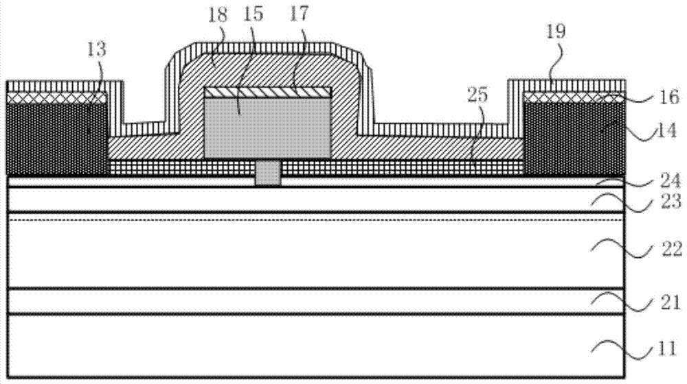
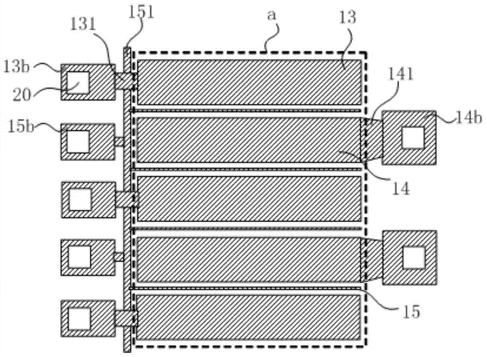
[0054] figure 1 A schematic cross-sectional structure diagram of a semiconductor device provided by Embodiment 1 of the present invention is shown, figure 2 It shows a schematic top view structure of the semiconductor device provided by Embodiment 1 of the present invention, combined with figure 1 with figure 2 Embodiment 1 of the present invention will be described.

[0055] See figure 1 with figure 2 , the semiconductor device includes: a substrate 11, a multilayer semiconductor layer on the substrate 11, the multilayer semiconductor layer includes an active region a and an inactive region, and the region outside the active region a is the inactive region , a source electrode and a drain electrode located on the multi-layer semiconductor layer, the source electrode and the drain electrode include a source electrode 13 and a drain electrode 14 located in the active region a and a source electrode 13b located in the passive region and the drain electrode 14b, the gate ...

Embodiment 2

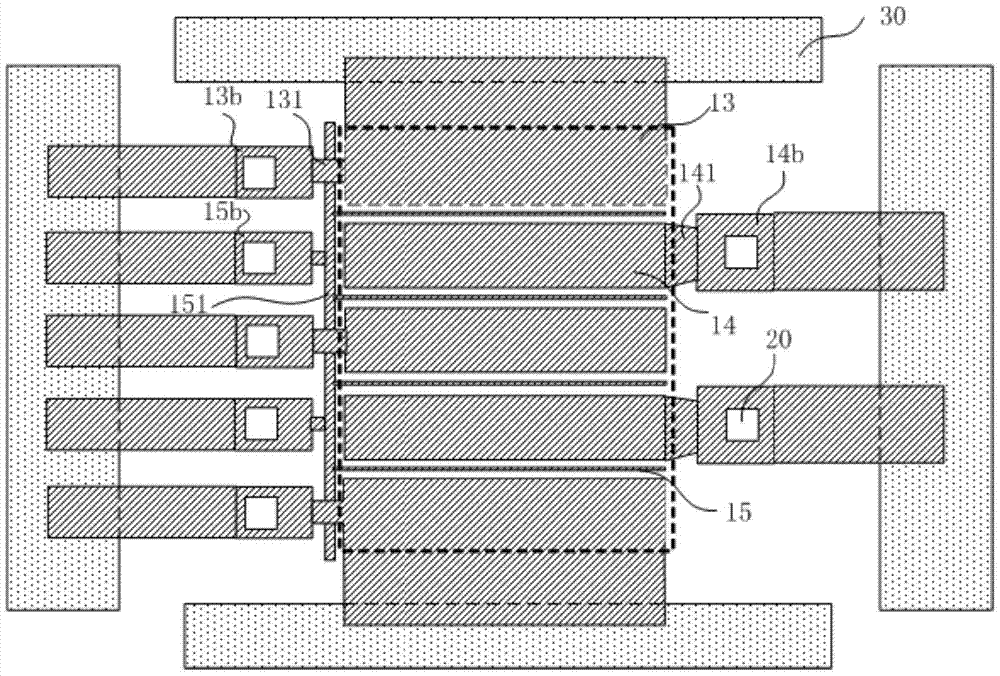
[0079] image 3 shows a schematic top view of the semiconductor device provided by Embodiment 2 of the present invention, Figure 4 shows a schematic diagram of the cross-sectional temperature of a semiconductor device in the prior art, Figure 5 It shows the cross-sectional temperature schematic diagram of the semiconductor device provided by the second embodiment of the present invention, combined with Figure 3 to Figure 5 Embodiment 2 of the present invention will be described.

[0080] The semiconductor device provided in Embodiment 2 of the present invention is based on the semiconductor device provided in Embodiment 1 above, and the same parts as the semiconductor device in Embodiment 1 will not be described again.

[0081] The semiconductor device provided by Embodiment 2 of the present invention further includes a heat sink 30 arranged around the edge of the passive area, and the second heat dissipation layer 16 is connected to the heat sink 30 .

[0082] In this e...

Embodiment 3

[0088] Image 6 A schematic diagram showing the cross-sectional structure of the active region of the semiconductor device provided by Embodiment 3 of the present invention, please refer to Image 6 , the semiconductor device includes: a substrate 11, a multilayer semiconductor layer positioned on the substrate 11, the multilayer semiconductor layer includes an active region a and a passive region ( Image 6 not shown in ), the area outside the active area a is an inactive area, and the source and drain electrodes located on the multi-layer semiconductor layer include the source electrode 13 located in the active area a and the drain electrode 14 and the source electrode 13b located in the passive region ( Image 6 Not shown in) and drain electrode 14b ( Image 6 not shown in ), the gate is located on the multi-layer semiconductor, and the gate is interdigitated between the source and the drain, and the gate includes a gate 15 located in the active region and a gate located ...


PUM


Abstract

The invention discloses a semiconductor device, comprising a substrate, a multi-layer semiconductor layer on the substrate, a multi-layer semiconductor layer including an active area and a passive area, a source electrode and a drain electrode located in the active area, and a passive area The source electrode and the drain electrode, the gate electrode on the active region and the gate electrode on the passive region, the source, drain and gate and / or the source electrode, drain electrode and gate electrode are provided with graphite vinyl thermal layer. Due to the excellent heat dissipation characteristics of graphene, it can accelerate the heat transfer of local heat sources along the lateral direction, increase the heat dissipation path of the device, thereby improve the heat dissipation effect of the semiconductor device, reduce the internal temperature of the semiconductor device, and improve the reliability of the semiconductor device.

Description

technical field [0001] The invention relates to the technical field of semiconductors, in particular to a semiconductor device. Background technique [0002] GaN semiconductor devices have significant advantages such as large band gap, high electron mobility, high breakdown field strength, and high temperature resistance. Compared with the first-generation semiconductor silicon and the second-generation semiconductor gallium arsenide, it is more suitable for making high-temperature, high-voltage, High-frequency and high-power electronic devices have broad application prospects. [0003] Since GaN semiconductor devices work in a high-power and high-current environment, the heat generated by GaN semiconductor devices is relatively high. Some structures in GaN semiconductor devices are greatly affected by temperature, such as Schottky contact and carrier mobility, etc. If local high temperature is generated at the Schottky contact, the Schottky contact will be degraded and the...

Claims


Application Information

Patent Timeline
Patent Type & Authority Patents(China)
IPC IPC(8): H01L23/367
CPCH01L29/452H01L29/475H01L29/7786H01L29/1606H01L29/2003H01L29/413H01L23/373H01L23/3736H01L2924/0002H01L29/4175H01L29/41758H01L29/40114H01L2924/00H01L29/0673H01L29/7787H01L2924/13064H01L29/0847H01L29/20
Inventor 裴轶周梦杰张乃千
Owner DYNAX SEMICON
Why Eureka
Try Eureka