a semiconductor device

A semiconductor and device technology, applied in the field of semiconductor devices, can solve problems such as poor heat dissipation of semiconductor devices, and achieve the effects of improving reliability, improving heat dissipation effect, and uniform thermal field distribution

Active Publication Date: 2020-06-05
GPOWER SEMICON
View PDF2 Cites 0 Cited by
  • Summary
  • Abstract
  • Description
  • Claims
  • Application Information

AI Technical Summary

Problems solved by technology

[0005] An embodiment of the present invention provides a semiconductor device to solve the problem of poor heat dissipation of semiconductor devices in the prior art

Method used


Image

  • a semiconductor device
  • a semiconductor device
  • a semiconductor device

Examples


Embodiment Construction

[0026] In order to make the purpose, technical solutions and advantages of the present invention clearer, the technical solutions of the present invention will be clearly and completely described through implementation with reference to the accompanying drawings in the embodiments of the present invention. Obviously, the described embodiments are the embodiment of the present invention. Some, but not all, embodiments. Based on the embodiments of the present invention, all other embodiments obtained by persons of ordinary skill in the art without making creative efforts belong to the protection scope of the present invention.

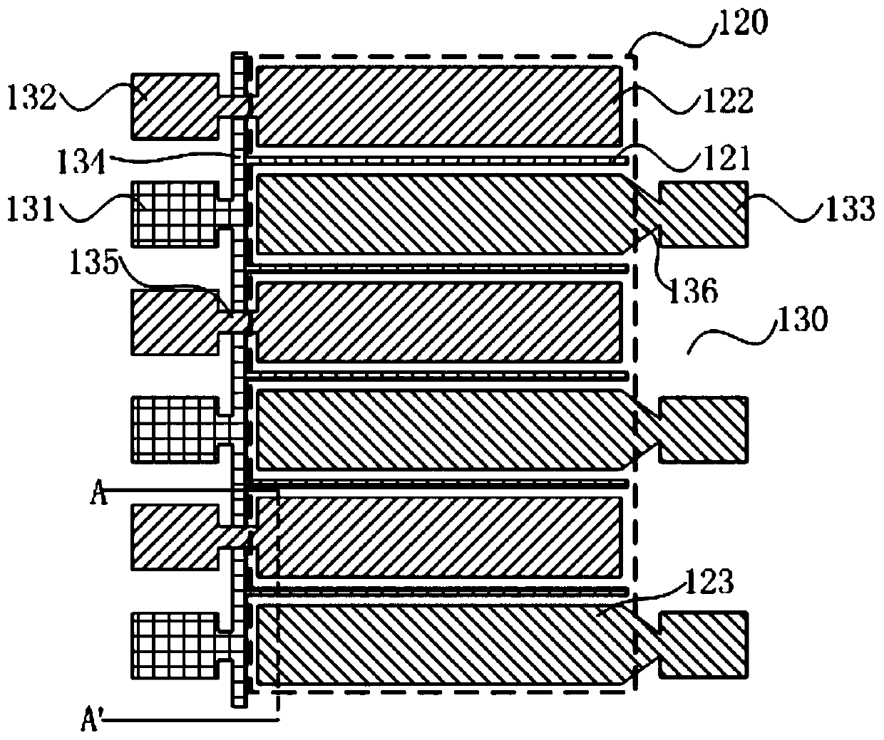
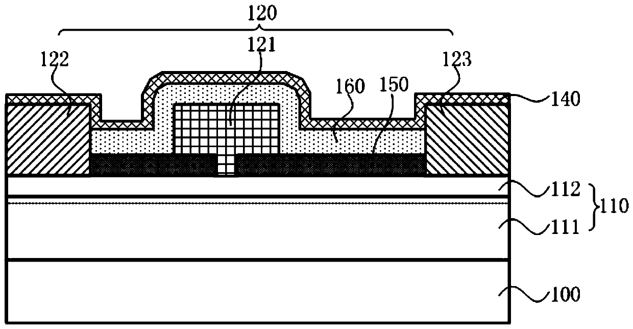
[0027] Figure 1A It is a top view of the semiconductor device provided by Embodiment 1 of the present invention, Figure 1B yes Figure 1A A cross-sectional view along A-A', where, Figure 1B dissected Figure 1A The structure of a transistor. The semiconductor device provided in this embodiment includes: a substrate 100; a multilayer semiconductor la...


PUM


Abstract

The embodiment of the present invention discloses a semiconductor device, which includes: a substrate; a multilayer semiconductor layer located on the substrate, an active region and a passive region located outside the active region are arranged on the multilayer semiconductor; a gate, a source, and a drain located within the active region; and a heat dissipation layer covering at least a portion of the active region and including a heat dissipation material. In the present invention, a heat dissipation layer covering at least a part of the active area is provided in the semiconductor device. The arrangement of the heat dissipation layer can increase the heat conduction path of the semiconductor device in the plane direction, and accelerate heat from the heat source inside the semiconductor device to the outside of the semiconductor device. Conduction, improve the heat dissipation effect of semiconductor devices, reduce the temperature inside the semiconductor device, make the thermal field distribution inside the semiconductor device more uniform, and improve the reliability of the semiconductor device.

Description

technical field [0001] Embodiments of the present invention relate to semiconductor technologies, and in particular, to a semiconductor device. Background technique [0002] Gallium nitride GaN semiconductor devices have significant advantages such as large band gap, high electron mobility, high breakdown field strength, and high temperature resistance. Compared with the first-generation semiconductor silicon and the second-generation semiconductor gallium arsenide, it is more suitable for making high-temperature , high voltage, high frequency and high power electronic devices have broad application prospects. [0003] GaN semiconductor devices usually work in a high-power and high-current environment, and the working conditions will cause high heat to be generated in the active region of the GaN semiconductor device, which will lead to an increase in the temperature of the device structure, and the increase in temperature will cause GaN semiconductor The performance of the...

Claims


Application Information

Patent Timeline
Patent Type & Authority Patents(China)
IPC IPC(8): H01L23/36H01L29/20
CPCH01L23/36H01L29/2003H01L23/291H01L29/4175H01L29/41758H01L29/7786H01L23/4824H01L23/4821H01L23/3738H01L29/78
Inventor 裴轶周梦杰
Owner GPOWER SEMICON
Why Eureka
Try Eureka