PCB splitting jig

A jig and split technology, applied in the processing of insulating substrates/layers, mechanical/acoustic circuit processing, electrical components, etc., can solve the problems of many board edges and low efficiency, reduce board edge burrs, improve The effect of shard efficiency

Inactive Publication Date: 2015-03-11
竞陆电子(昆山)有限公司
View PDF0 Cites 1 Cited by
  • Summary
  • Abstract
  • Description
  • Claims
  • Application Information

AI Technical Summary

Problems solved by technology

At present, the operator breaks off the small PCB pieces on the joint printed circuit b...

Method used


Image

  • PCB splitting jig
  • PCB splitting jig
  • PCB splitting jig

Examples


Embodiment

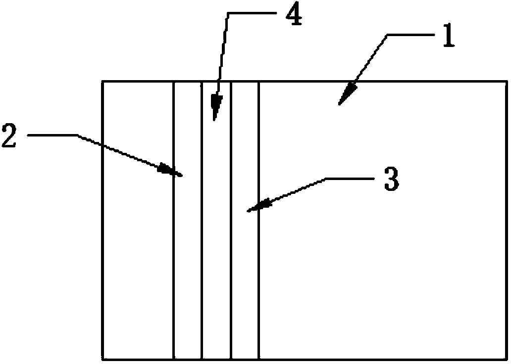
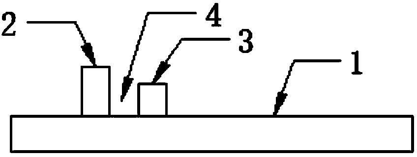
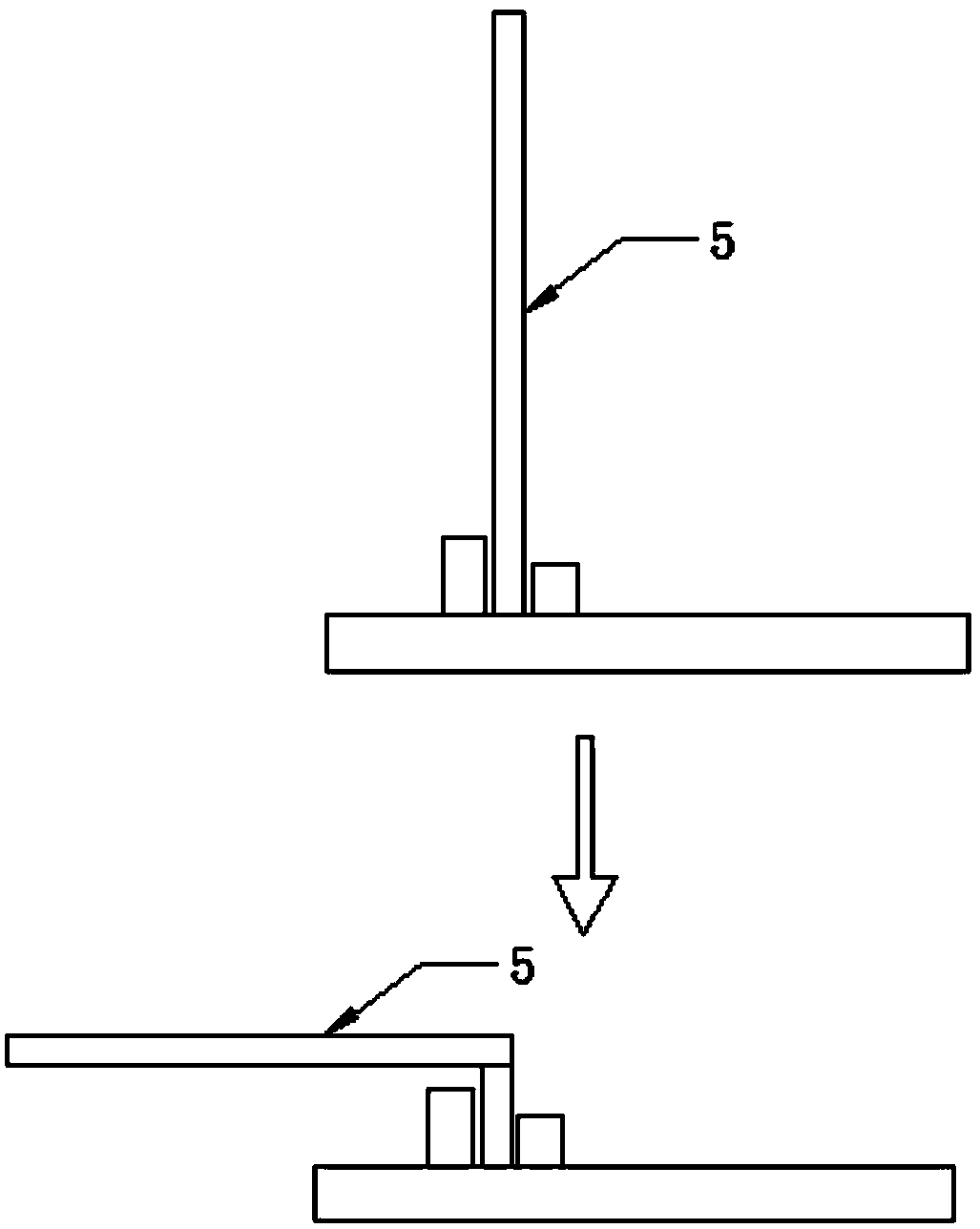
[0020] Embodiment: a kind of PCB splinter fixture, such as figure 1 and figure 2 As shown, it is composed of a working panel 1, a left side panel 2 and a right side panel 3. The working panel is a flat plate arranged horizontally, and the left side panel and the right side panel are all fixed on the upper surface of the working panel. The left side plate and the right side plate are parallel to each other, and there is a gap between the left side plate and the right side to form a slit 4, the width of the slit is greater than the thickness of the joint printed circuit board, and the left side plate The upper surface of the upper surface is higher than the upper surface of the right side board and the height difference is 3 millimeters, and the thickness of the left side board is less than the length and width of the single PCB.

[0021] The specific size of this PCB split fixture is that the thickness of the working panel is 10 millimeters, the thickness of the left side pla...


PUM

PropertyMeasurementUnit
Thicknessaaaaaaaaaa
Thicknessaaaaaaaaaa
Lengthaaaaaaaaaa

Abstract

The invention discloses a PCB splitting jig. The PCB splitting jig is composed of a working panel, a left side plate and a right side plate; the working panel is a flat panel arranged horizontally; the left side plate and the right side plate both are fixed on the upper surface of the working panel and are parallel to each other, a gap is formed between the left side plate and the right side plate to form a slot, and the width of the slot is greater than the thickness of a joint printed circuit board; the upper surface of the left side plate is higher than the upper surface of the right side plate and the height different is 2-5mm; the thickness of the left side plate is small than the length and the width of a single PCB. The PCB splitting jig is capable of splitting the small single PCBs on the joint printed circuit board row by row, and therefore, the splitting efficiency is greatly improved and burrs at the edges of the boards are reduced; the PCB splitting jig is simple in structure and easy to implement.

Description

technical field [0001] The invention belongs to the field of equipment for manufacturing printed circuit boards, and in particular relates to a splinter jig for separating small PCBs on a joint printed circuit board. Background technique [0002] The joint printed circuit board is to produce multiple small PCB single-pieces at the same time to form a large joint printed circuit board composed of many small PCB single-pieces, but these small PCB single-pieces need to be used separately when used The, therefore, need to separate them piece by piece. At present, the operator manually breaks off the small PCBs on the joint printed circuit board one by one, which is not only inefficient, but also has many burrs on the edge of the board. Contents of the invention [0003] In order to solve the above problems, the present invention provides a PCB split fixture, which can easily and simply break apart the small PCB single pieces on the joint printed circuit board, greatly improvi...

Claims


Application Information

Patent Timeline
IPC IPC(8): H05K3/00
CPCH05K3/0052H05K2203/02
Inventor 李泽清
Owner 竞陆电子(昆山)有限公司
Why Eureka
Try Eureka