Thin film transistor array substrate, manufacturing method thereof and displaying device

A thin-film transistor and array substrate technology, applied in the field of liquid crystal display, can solve problems such as poor display, increased surface unevenness, and easy peeling off of PI film, and achieve the effects of improving display performance, improving surface unevenness, and increasing adhesion

Inactive Publication Date: 2015-03-25
TCL CHINA STAR OPTOELECTRONICS TECH CO LTD
View PDF7 Cites 9 Cited by
  • Summary
  • Abstract
  • Description
  • Claims
  • Application Information

AI Technical Summary

Problems solved by technology

[0005] The technical problem to be solved by the present invention is: in the manufacturing process of the thin film transistor array substrate of the In Cell type embedded touch display panel in the prior art, due to the existence of the touch metal layer, the surface of the array substrate before coating PI will be The increase of unevenness makes the coated PI film easy to fall off, resulting in poor display

Method used


Image

  • Thin film transistor array substrate, manufacturing method thereof and displaying device
  • Thin film transistor array substrate, manufacturing method thereof and displaying device
  • Thin film transistor array substrate, manufacturing method thereof and displaying device

Examples


Embodiment Construction

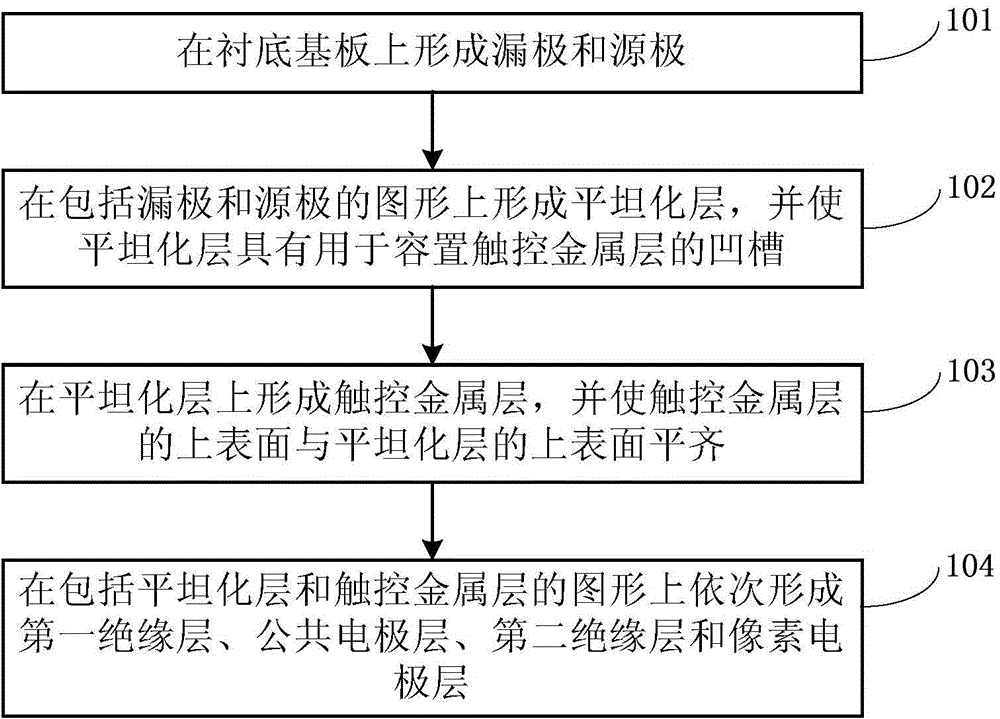
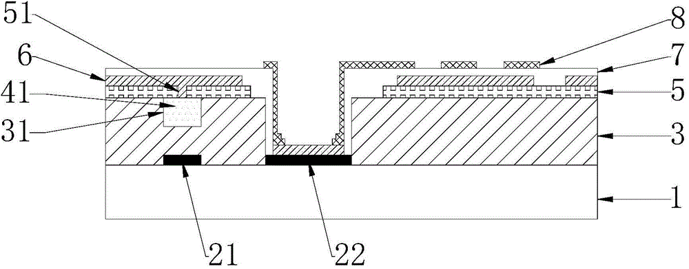
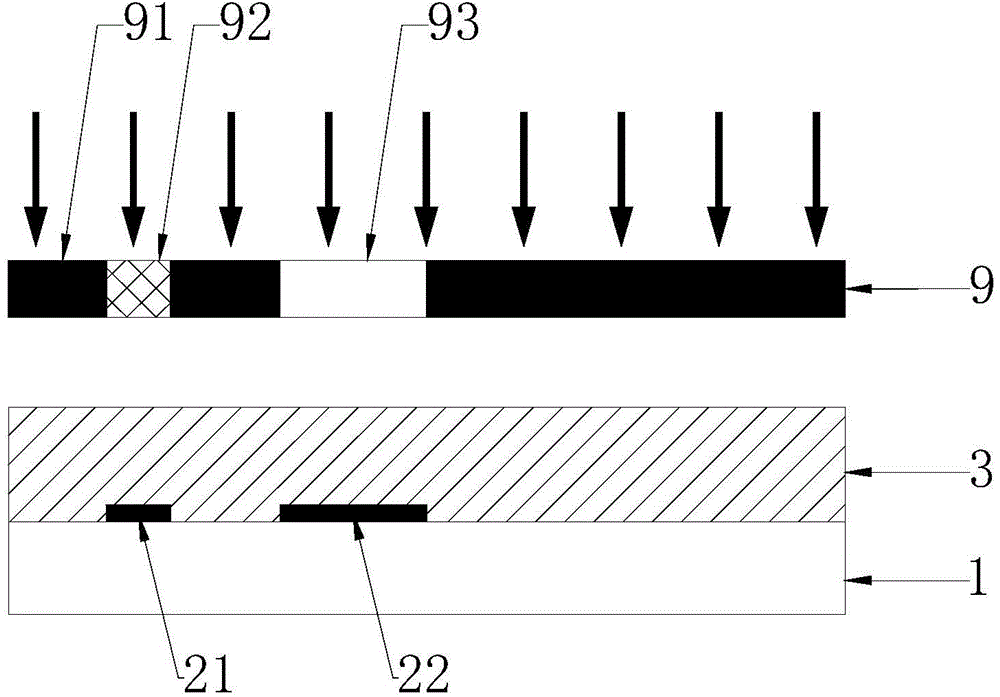
[0046] The implementation of the present invention will be described in detail below in conjunction with the accompanying drawings and examples, so as to fully understand and implement the process of how to apply technical means to solve technical problems and achieve technical effects in the present invention. It should be noted that, as long as there is no conflict, each embodiment and each feature in each embodiment of the present invention can be combined with each other, and the formed technical solutions are all within the protection scope of the present invention.

[0047] The technical problem to be solved by the present invention is: in the manufacturing process of the thin film transistor array substrate of the In Cell type embedded touch display panel in the prior art, due to the existence of the touch metal layer, the surface of the array substrate before coating PI will be The increase of the degree of unevenness makes the coated PI film easy to fall off, resulting...


PUM


Abstract

The invention discloses a thin film transistor array substrate, a manufacturing method thereof and a displaying device. The method comprises the steps that a drain electrode and a source electrode are formed on a substrate; a planarization layer with a groove is formed; a touch metal layer with the upper surface flush with the upper surface of the planarization layer is formed; and a first insulation layer, a common electrode layer, a second insulation layer and a pixel electrode layer are formed. The surface concave-convex degree of the thin film transistor array substrate is improved, the adhesiveness between a PI film and the array substrate is improved, and the displaying performance of the displaying device is improved.

Description

technical field [0001] The present invention relates to the technical field of liquid crystal display, in particular to a thin film transistor array substrate and a manufacturing method thereof, and also relates to a display device with the thin film transistor array substrate. Background technique [0002] The manufacture of a general TFT-LCD (Thin Film Transistor-Liquid Crystal Display, Thin Film Transistor-Liquid Crystal Display) is completed through the following three steps: TFT array substrate manufacturing steps, CF (color filter plate) substrate manufacturing steps, and liquid crystal formation. Box (Cell) manufacturing steps. Among them, when forming a liquid crystal cell, the alignment of liquid crystal molecules is mainly carried out by coating PI (polyimide) on the TFT side substrate (ie, TFT array substrate) and the CF side substrate respectively, so that the liquid crystal molecules are in a natural state. It is at a specific angle, and after that liquid cryst...

Claims


Application Information

Patent Timeline
Patent Type & Authority Applications(China)
IPC IPC(8): G02F1/1333G06F3/041
CPCG02F1/13338G02F1/136227G02F1/1368G06F3/0412G06F2203/04103G02F1/136295H01L27/1214H01L27/1259G02F1/1333
Inventor 杜海波申智渊明星占伟虞晓江
Owner TCL CHINA STAR OPTOELECTRONICS TECH CO LTD
Why Eureka
Try Eureka